A manufacturing method for a backside-illumination sensor

A sensor, back-illuminated technology, applied in the field of preparation of back-illuminated sensors, can solve the problems of photon loss, affect the appearance of the wafer, affect the QE and imaging quality, and achieve the effect of reducing the difference

Active Publication Date: 2016-06-22
WUHAN XINXIN SEMICON MFG CO LTD
View PDF6 Cites 4 Cited by
  • Summary
  • Abstract
  • Description
  • Claims
  • Application Information

AI Technical Summary

Problems solved by technology

[0003] The back-illuminated image sensor wafers prepared by the current process show serious color abnormalities in appearance, which not only affects the appearance of the wafers, but also may cause differences in the loss of photons in the optical path, thereby affecting QE and Imaging quality, which is not expected by those skilled in the art

Method used


Image

  • A manufacturing method for a backside-illumination sensor
  • A manufacturing method for a backside-illumination sensor
  • A manufacturing method for a backside-illumination sensor

Examples


Embodiment Construction

[0026] The present invention will be further described below in conjunction with the accompanying drawings and specific embodiments, but not as a limitation of the present invention.

[0027] Such as figure 1 As shown, this embodiment relates to a method for preparing a back-illuminated sensor, which may be a back-illuminated image sensor. Specifically, the method includes the following steps:

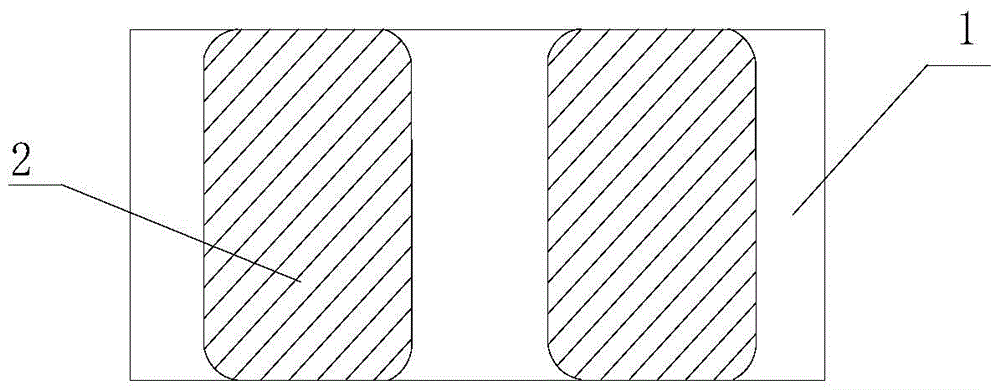
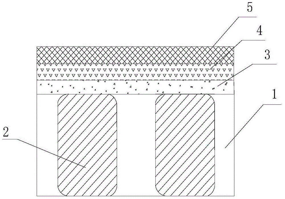
[0028] Step S1, providing a semiconductor substrate 1 with a front side and a back side, and a photodiode array (pixel array) formed by several photodiodes 2 (pixels) is formed in the semiconductor substrate 1; in an embodiment of the present invention, the The semiconductor substrate 1 is a wafer that has completed all the processes before the BSI process; the next process is to define the position of each pixel (photodiode) on the wafer for subsequent formation of color filters (colorfilter) process needs, such as figure 2 structure shown.

[0029] Step S2, forming a metal grid l...


PUM


Abstract

The invention relates to the technical field of semiconductor manufacturing, and especially relates to a manufacturing method for a backside-illumination sensor. A metal grid layer, a first oxide layer and a barrier layer sequentially form from bottom to top on the back surface of a semiconductor substrate; after a process of forming several metal grids through etching, a second oxide layer, of which the upper surface is level with the upper surface of the barrier layer, forms; and then, the barrier layer and the second oxide layer positioned on the first oxide layer are removed to form an oxide layer positioned on the upper surface of the metal grid layer and having uniform thickness. Difference of incident light losses is reduced, so that color abnormity of the appearance of a wafer of the backside-illumination sensor can be eliminated and the imaging quality can be raised.

Description

technical field [0001] The invention relates to the technical field of semiconductor manufacturing, in particular to a preparation method of a back-illuminated sensor. Background technique [0002] With the rapid development of semiconductor technology, semiconductor devices are used in various electronic applications such as personal computers, mobile phones, digital cameras, and other electronic equipment. Among them, a backside illuminated (BSI) sensor is a CMOS image sensor in which light enters the substrate from the backside of the substrate instead of the front side. And due to the use of backside illumination technology (BSI), the reading circuit and interconnection on the optical path are effectively removed, the loss of light in the intermediate link is reduced, and higher quantum efficiency (quantum efficiency (QuantumEfficiency, QE) refers to the incident to Among the photons on the surface of the photodiode, the proportion of the photogenerated electrons finall...

Claims


Application Information

Patent Timeline
Patent Type & Authority Applications(China)
IPC IPC(8): H01L27/146
CPCH01L27/1462H01L27/1464H01L27/14685
Inventor 王前文胡胜胡思平董金文
Owner WUHAN XINXIN SEMICON MFG CO LTD
Why Eureka
Try Eureka