Superjunction and method of making the same

A manufacturing method and super junction technology, applied in semiconductor devices, electrical components, circuits, etc., can solve the problems of weak electromagnetic interference performance and fast switching speed of devices, so as to improve the time of complete reverse bias, reduce on-resistance, The effect of etch and fill process simplicity

Active Publication Date: 2018-10-26
SHANGHAI HUAHONG GRACE SEMICON MFG CORP
View PDF4 Cites 0 Cited by
  • Summary
  • Abstract
  • Description
  • Claims
  • Application Information

AI Technical Summary

Problems solved by technology

The disadvantage of the super junction formed by this method is that it will cause the device switching speed to have a faster value, resulting in weaker electromagnetic interference performance (EMI) performance

Method used


Image

  • Superjunction and method of making the same
  • Superjunction and method of making the same
  • Superjunction and method of making the same

Examples


Embodiment Construction

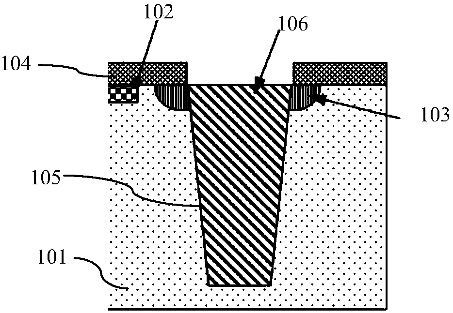
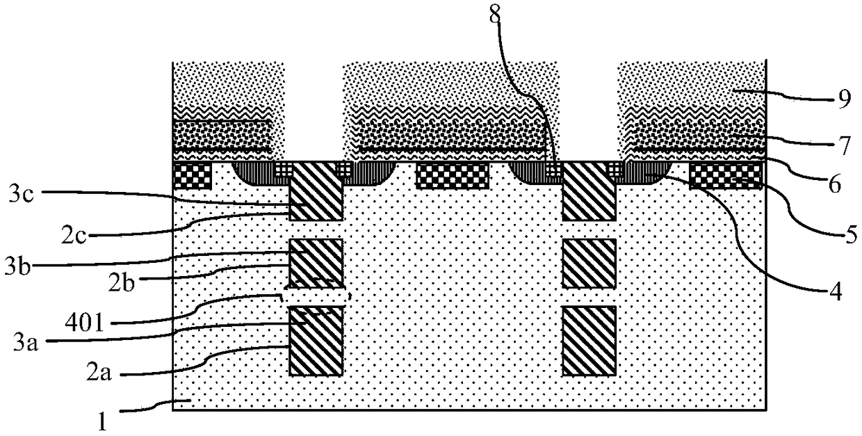
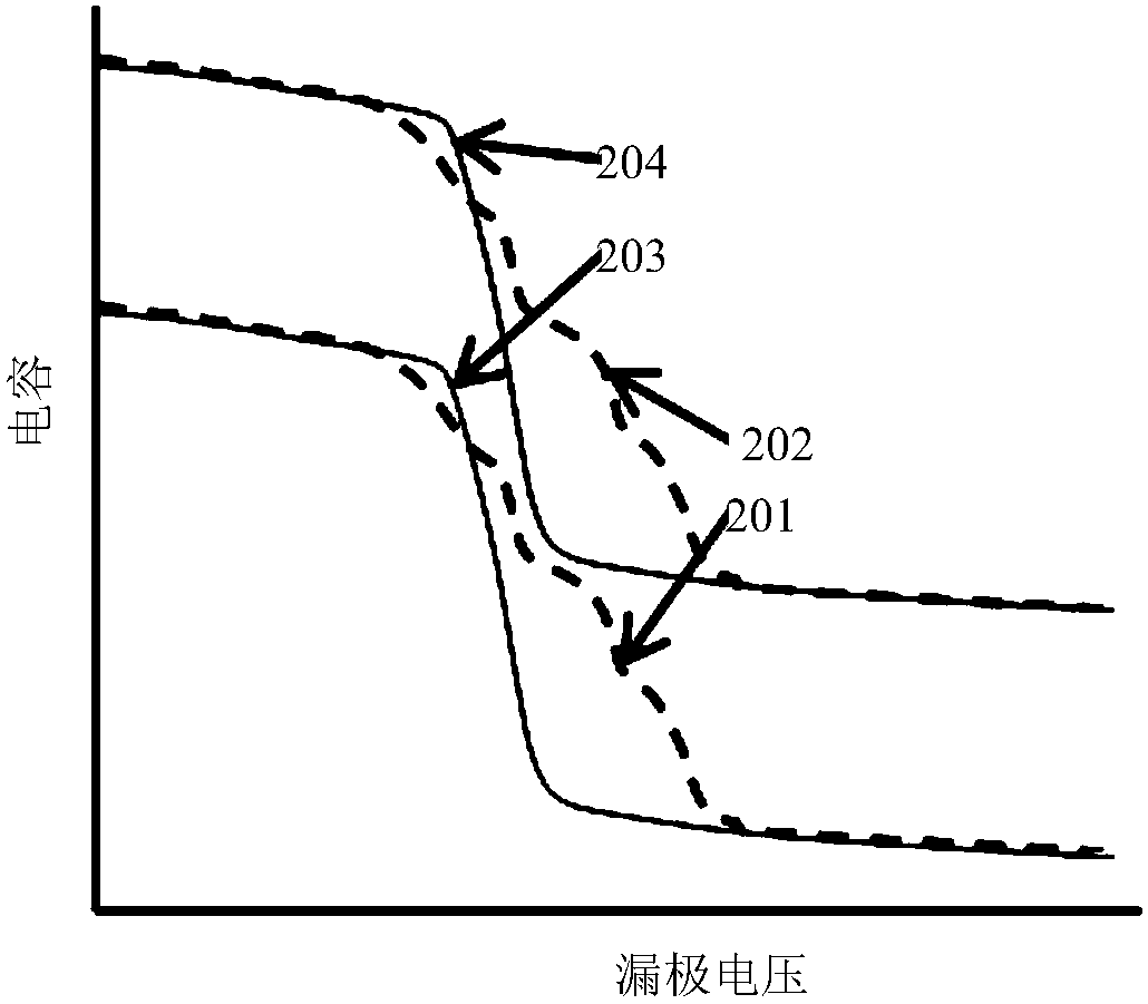
[0047] First of all, let me explain the EMI problem caused by the continuous improvement of the super junction process: the current mass production process has a diffusion resistance (RSP) close to 10mohm cm 2 . This brings about a substantial reduction in device area, which is a huge advantage in terms of manufacturing costs. However, due to the sharp reduction of device area, some other problems have also been brought about, and EMI problem is one of them. EMI is due to the fact that after the device is reduced, all parasitic capacitances are also reduced due to the reduction in area, resulting in a sharp increase in device switching speed, higher dV / dt, dI / dt is very easy to cause oscillations in the parasitic capacitance and inductance in the circuit, resulting in Excessive electromagnetic radiation, that is, EMI problem. In the existing method, the EMI problem of the super junction device formed by trench filling is more prominent than that of the super junction device ...


PUM


Abstract

The invention discloses a super junction. The super junction is formed by more than two super junction sub layers in a superposition manner; sub trenches are formed in N type epitaxy sub layers in each super junction sub layer; each P type sub thin layer is formed by P type epitaxy sub layers filled in the sub trenches; each N type sub thin layer is formed by N type epitaxy sub layers among the sub trenches; the sub trenches of each super junction sub layer are longitudinally aligned; the P type sub thin layers are longitudinally overlapped to form a P type thin layer; the N type sub thin layers are longitudinally overlapped to form an N type thin layer; and the doping concentrations and thicknesses of the N type epitaxy sub layers among the super junction sub layers, the depths of the sub trenches, and the doping concentrations of the P type epitaxy sub layers are singly and separately set, so that the widths of the depletion layers among the super junction sub layers adopt a layered structure. The invention also discloses the super junction and a manufacturing method for the super junction. The switching speed of a device formed by the super junction can be lowered, so that the external electromagnetic interference property of the super junction device is lowered as well.

Description

technical field [0001] The invention relates to the field of manufacturing semiconductor integrated circuits, in particular to a super junction; the invention also relates to a method for manufacturing the super junction. Background technique [0002] The super junction is composed of alternately arranged P-type thin layers and N-type thin layers formed in the semiconductor substrate. There are two existing super junction methods: the first is multiple epitaxy with multiple ion implantations, and then The multiple implanted P-type wells (well) are connected into a P-type pillar, that is, a P-type thin layer by a drivein method, which can control the improvement of electromagnetic interference performance (EMI) through the concentration of ion implantation. [0003] Another approach is to first grow one or more layers of epitaxy, hollow out the trenches (Trench) that need to be filled with P-type pillars by digging trenches, and then fill them with P-type epitaxy to form P-ty...

Claims


Application Information

Patent Timeline
Patent Type & Authority Patents(China)
IPC IPC(8): H01L29/06
CPCH01L29/0688
Inventor 冯海浪祝志敏王飞
Owner SHANGHAI HUAHONG GRACE SEMICON MFG CORP
Why Eureka
Try Eureka