A quantum-tailored transparent electrode for crystalline silicon solar cells

A technology of solar cells and transparent electrodes, applied in the field of solar cells, can solve the problems of high cost, reduced cell conversion efficiency, high material cost, etc., and achieves the effect of expanding the spectrum utilization range, improving the photoelectric conversion efficiency, and simplifying the production process.

Active Publication Date: 2017-10-24
LONGI SOLAR TECH CO LTD
View PDF3 Cites 0 Cited by
  • Summary
  • Abstract
  • Description
  • Claims
  • Application Information

AI Technical Summary

Problems solved by technology

At present, there are two problems that need to be solved urgently: the first is that the spectral response of crystalline silicon solar cells is poorly matched with the solar spectrum, and most of the light energy in the solar spectrum cannot be utilized; the second is the metal electrodes on the front and back of crystalline silicon solar cells light shading and high cost issues
[0005] The light-receiving surface electrodes of conventional crystalline silicon cells are screen-printed with silver paste to form nearly a hundred fine grids and several main grids. The materials used in this process are expensive, and silver electrodes will cause 5% to 7% of the surface of the cell The area forms a light shield, which greatly reduces the conversion efficiency of the cell

Method used


Image

  • A quantum-tailored transparent electrode for crystalline silicon solar cells
  • A quantum-tailored transparent electrode for crystalline silicon solar cells
  • A quantum-tailored transparent electrode for crystalline silicon solar cells

Examples


Embodiment 1

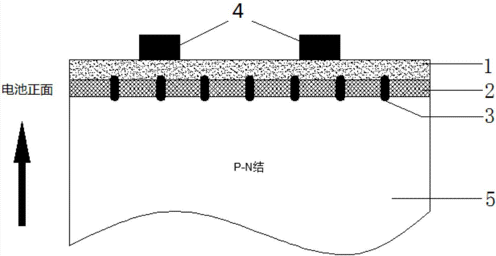
[0036] (1) P-type monocrystalline silicon wafers are processed through processes such as texturing, diffusion, etching, deposition of passivation film and anti-reflection film, and production of back electrodes;

[0037] (2) adopt screen printing method to make dotted silver electrode on the front, the diameter of single dot is 50um, and the distance between dot and dot is 0.8mm;

[0038] (3) Carry out sintering at 300-900°C in the furnace body, and the dotted silver paste on the front side penetrates the anti-reflection film and passivation film to form a good ohmic contact with the silicon substrate;

[0039] (4) Prepare a 100nm doped AZO transparent conductive film by sputtering on the dot electrode, and the doping element is Eu 3+ , the mass fraction of doping is 0.001%;

[0040] (5) On the doped AZO transparent conductive film, adopt the method of screen printing to make silver electrodes. The silver electrode pattern is composed of a group of equidistant parallel grid l...

Embodiment 2

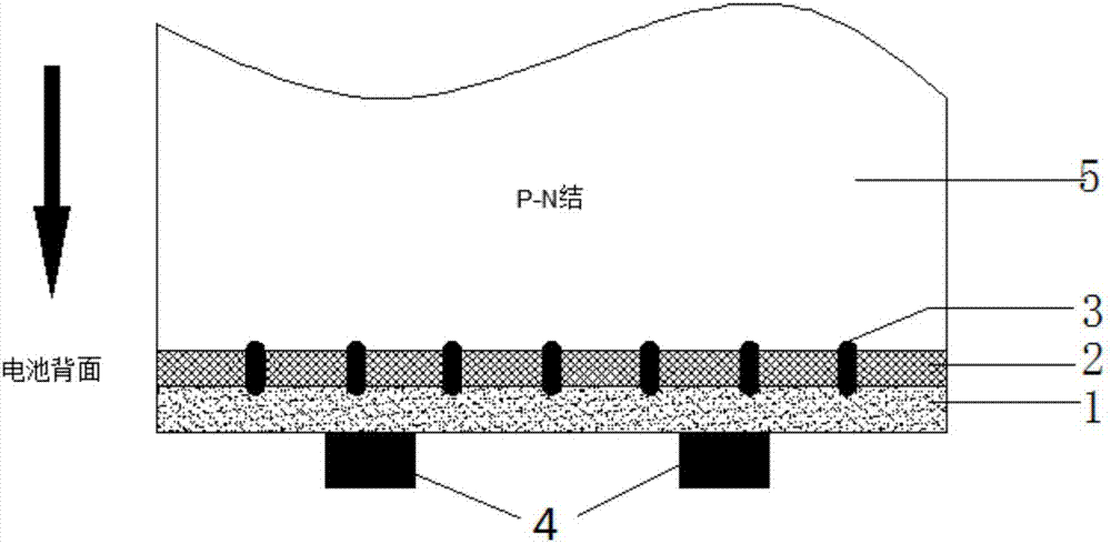
[0042] (1) N-type monocrystalline silicon wafers are processed through processes such as texturing, diffusion, etching, deposition of passivation film and anti-reflection film;

[0043] (2) Laser is used to open the anti-reflection film and passivation film on the front and back in a point array, the diameter of a single point is 100um, and the distance between points is 1.5mm;

[0044] (3) Prepare dot-shaped aluminum electrodes and silver electrodes at the openings on the front and back sides by electroless plating, and then perform annealing treatment at 200-500°C;

[0045] (4) Prepare a 110nm doped ITO transparent conductive film by chemical vapor deposition on the front side, and the doping element is Bi 3+ and Sm 3+ , the total mass fraction of doping is 0.01%;

[0046] (5) Prepare a 110nm doped ITO transparent conductive film by chemical vapor deposition on the back, and the doping element is Yb 3+ and Er 3+ , the total mass fraction of doping is 0.01%;

[0047] (6)...

Embodiment 3

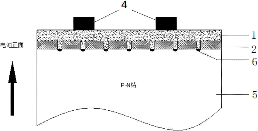
[0050] (1) P-type monocrystalline silicon wafers are processed through processes such as texturing, diffusion, etching, deposition of passivation film and anti-reflection film;

[0051] (2) Print phosphorus-containing dopants and boron-containing dopants on the front and back according to specific patterns, the printed pattern adopts a line segment array, the length of the line segment is 50um, the width is 40um, and the distance between the line segments is 0.5mm;

[0052] (3) Use laser to pulse heat the dopant according to the specific pattern described in step (2), so that phosphorus atoms and boron atoms penetrate the anti-reflection film and passivation film to diffuse to the silicon substrate, on the front side of the silicon wafer and A locally heavily doped region forming a line-segment array on the back;

[0053] (4) Spray doped FTO nanopowder on the front to form a doped transparent conductive film with a thickness of 200nm, and the doping element is Eu 3+ , the ma...


PUM


Abstract

The invention provides a quantum clipped transparent electrode for a crystalline silicon solar cell. A doped transparent conductive film provided by the invention can partially contact with metal or heavy doped areas which are distributed in an array mode, thus forming the front or back electrode of the crystalline silicon solar cell. According to the electrode provided by the invention, the spectrum utilization range of the crystalline silicon solar cell is expanded; and the photoelectric conversion efficiency of the battery is greatly improved.

Description

technical field [0001] The invention belongs to the technical field of solar cells, in particular to a quantum tailoring transparent electrode for crystalline silicon solar cells. Background technique [0002] Since the first solar cell was born in Bell Laboratories in 1954, crystalline silicon solar cells have been widely used, the conversion efficiency has been continuously improved, and the production cost has continued to decline. At present, crystalline silicon solar cells account for more than 80% of the total global solar cell market, and the conversion efficiency of crystalline silicon cell production lines has exceeded 20%. The cost of electricity continues to shrink and is expected to be flat in the next few years. As a clean energy source, crystalline silicon solar cells play an increasingly important role in changing the energy structure and alleviating environmental pressure. [0003] If crystalline silicon solar cells want to continue to maintain their compet...

Claims


Application Information

Patent Timeline
Patent Type & Authority Patents(China)
IPC IPC(8): H01L31/0224H01L31/068H01L31/055
CPCH01L31/022425H01L31/022466H01L31/055H01L31/068Y02E10/52Y02E10/547
Inventor 赵科雄李华
Owner LONGI SOLAR TECH CO LTD
Why Eureka
Try Eureka