Manufacturing method of TFT substrate and manufactured TFT substrate

一种制作方法、基板的技术,应用在半导体/固态器件制造、半导体器件、电气元件等方向,能够解决影响电流、TFT结构不对称性等问题,达到避免电流通路的影响、实现对称性、降低关态电流的效果

Active Publication Date: 2016-07-06
TCL CHINA STAR OPTOELECTRONICS TECH CO LTD
View PDF3 Cites 3 Cited by
  • Summary
  • Abstract
  • Description
  • Claims
  • Application Information

AI Technical Summary

Problems solved by technology

However, in an LTP STFT, when the source electrode and the drain electrode adopt the offset and overlap structures respectively, it will cause the asymmetry of the TFT structure. characteristics which affect the current flowing through the device

Method used


Image

  • Manufacturing method of TFT substrate and manufactured TFT substrate
  • Manufacturing method of TFT substrate and manufactured TFT substrate
  • Manufacturing method of TFT substrate and manufactured TFT substrate

Examples


Embodiment Construction

[0044] In order to further illustrate the technical means adopted by the present invention and its effects, the following describes in detail in conjunction with preferred embodiments of the present invention and accompanying drawings.

[0045] see figure 1 , the invention provides a kind of manufacturing method of TFT substrate, comprises the following steps:

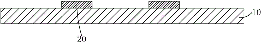
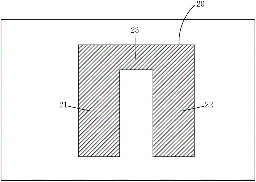
[0046] Step 1, such as Figure 2-3 As shown, a substrate 10 is provided, and a gate 20 is formed on the substrate 10. The gate 20 is a U-shaped structure, including a first vertical portion 21, a second vertical portion 22, and connecting the first and second vertical portions. The two vertical portions 21, 22 correspond to the transverse connecting portion 23 at the end.

[0047] Specifically, the preparation method of the gate 20 may be as follows: depositing a metal layer on the substrate 10 and patterning the metal layer with a photomask to obtain the gate 20 .

[0048] Specifically, the material of the metal la...


PUM


Abstract

The invention provides a manufacturing method of a TFT substrate and the manufactured TFT substrate. A first channel region and a first lightly doped compensation region are arranged between a first source and a drain; a second channel region and a second lightly doped compensation region are arranged between a second source and the drain; and a first overlapping region and a second overlapping region are formed between the drain and a gate and between the second source and the gate respectively, so that the paths through which currents flowing to the drain from the first source and the second source pass are the same as those through which the currents flowing to the first source and the second source from the drain pass, namely the paths of the currents from the sources to the drain and from the drain to the sources are the same; the symmetry of the TFT structure is achieved; the current flowing through a TFT device is not affected even if the drain and the sources are exchanged for use in practical work; and the electrical properties of the TFT device are improved.

Description

technical field [0001] The invention relates to the field of display technology, in particular to a method for manufacturing a TFT substrate and the prepared TFT substrate. Background technique [0002] OLED is a flat panel display technology with great development prospects. It has excellent display performance, especially self-illumination, simple structure, ultra-thin, fast response, wide viewing angle, low power consumption and flexible display. Known as the "dream display", coupled with the fact that its production equipment investment is much smaller than that of TFT-LCD, it has been favored by major display manufacturers and has become the main force of the third-generation display devices in the field of display technology. At present, OLED is on the eve of mass production. With the further deepening of research and the continuous emergence of new technologies, OLED display devices will surely have a breakthrough development. [0003] According to the driving method...

Claims


Application Information

Patent Timeline
Patent Type & Authority Applications(China)
IPC IPC(8): H01L27/12H01L21/77
CPCH01L21/77H01L27/1214H01L27/1259H01L29/66765H01L29/78624H01L29/78645H01L29/78678H01L21/02667H01L29/6675H01L29/786
Inventor 迟世鹏
Owner TCL CHINA STAR OPTOELECTRONICS TECH CO LTD
Why Eureka
Try Eureka