Substrate, manufacturing method thereof, and display device

A substrate and display area technology, which is applied in semiconductor/solid-state device manufacturing, electrical components, electric solid-state devices, etc., can solve problems such as poor display, weak antistatic ability, and electrostatic damage

Active Publication Date: 2016-07-20
BEIJING BOE DISPLAY TECH CO LTD +1
View PDF3 Cites 7 Cited by
  • Summary
  • Abstract
  • Description
  • Claims
  • Application Information

AI Technical Summary

Problems solved by technology

[0004] figure 1 In the array substrate shown in , the end of the idle line 13 facing the conductive connection structure 14 often forms a tip discharge phenomenon, and the conductive connection structure 14 is generally made o

Method used


Image

  • Substrate, manufacturing method thereof, and display device
  • Substrate, manufacturing method thereof, and display device
  • Substrate, manufacturing method thereof, and display device

Examples


Embodiment Construction

[0026] In order to understand the above-mentioned purpose, features and advantages of the present invention more clearly, the present invention will be further described in detail below in conjunction with the accompanying drawings and specific embodiments. It should be noted that, in the case of no conflict, the embodiments of the present application and the features in the embodiments can be combined with each other.

[0027] In the following description, many specific details are set forth in order to fully understand the present invention. However, the present invention can also be implemented in other ways different from those described here. Therefore, the protection scope of the present invention is not limited by the specific details disclosed below. EXAMPLE LIMITATIONS.

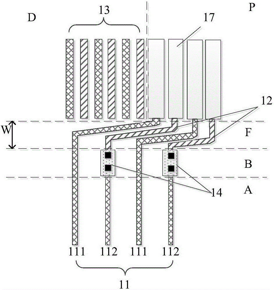
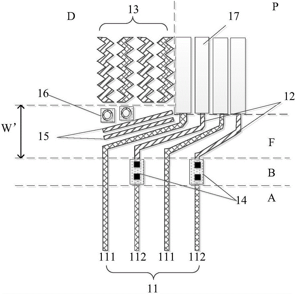
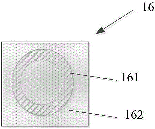
[0028] The structure of an embodiment of the substrate provided by the first aspect of the present invention can refer to figure 2 , for the convenience of description, the base included in the sub...


PUM


Abstract

The invention relates to a substrate, a manufacturing method thereof, and a display device. The substrate comprises at least one idle line, wherein the idle line comprises at least one tip, and the tip is suitable for discharging static electricity to the interior of an idle region. Therefore, the electrostatic charges generated at corresponding regions can be discharged to the idle region, thereby reducing static content discharged to a conductive connecting structure by the idle line, and reducing the risk that the conductive connecting structure is damaged by static electricity.

Description

technical field [0001] The invention relates to a substrate, a manufacturing method thereof, and a display device. Background technique [0002] The current display devices are generally assembled and packaged by a plurality of substrates, and some of the substrates (for example, array substrates fabricated with thin film transistors) need to be driven by external driving signals. These external signals are generally transmitted to the inside of the substrate through signal lines provided on the substrate. Due to the limited size of the driver chip that generates these external signals, generally the signal lines are collectively connected to the driver chip at the edge area of ​​the substrate. [0003] see figure 1 , is a structural schematic diagram of a partial structure of an array substrate in the prior art. The array substrate can be divided into five regions, namely display region A, bridging region B, fan-out region F (with a width of W), and idle region D and the...

Claims


Application Information

Patent Timeline
IPC IPC(8): H01L23/60H01L21/71
CPCH01L23/60H01L21/71
Inventor 李洋封宾唐硕孙鹏
Owner BEIJING BOE DISPLAY TECH CO LTD
Why Eureka
Try Eureka