A kind of PCB manufacturing method and PCB

A production method and PCB board technology, applied in the field of PCB and PCB production, can solve problems such as difficult to ensure the pass rate of fine lines, and achieve the effects of shortening the etching time, increasing the pass rate, and reducing side erosion

Active Publication Date: 2018-11-02
SHENNAN CIRCUITS
View PDF4 Cites 0 Cited by
  • Summary
  • Abstract
  • Description
  • Claims
  • Application Information

AI Technical Summary

Problems solved by technology

However, when using the existing manufacturing process to make fine lines, it is difficult to ensure the pass rate of fine lines due to the influence of side erosion on the line pattern

Method used


Image

  • A kind of PCB manufacturing method and PCB
  • A kind of PCB manufacturing method and PCB
  • A kind of PCB manufacturing method and PCB

Examples


Embodiment Construction

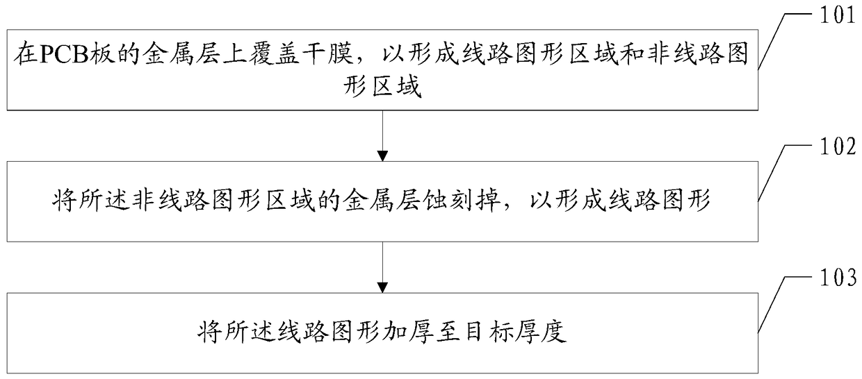
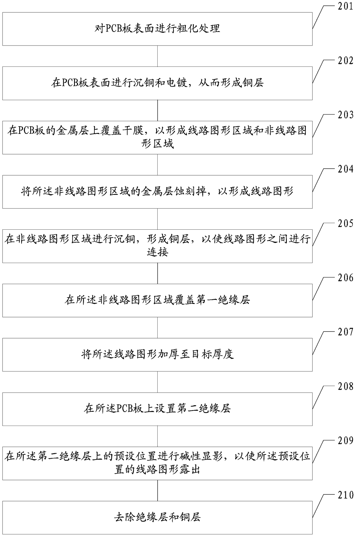
[0024] Embodiments of the present invention provide a method for manufacturing a PCB and the PCB, which are used to reduce the influence of side erosion in the process of making circuit patterns, and are suitable for making fine circuits.

[0025] The following will clearly and completely describe the technical solutions in the embodiments of the present invention with reference to the accompanying drawings in the embodiments of the present invention. Obviously, the described embodiments are only some, not all, embodiments of the present invention. Based on the embodiments of the present invention, all other embodiments obtained by those skilled in the art without creative efforts fall within the protection scope of the present invention. ,

[0026] It should be noted that the terms used in the embodiments of the present invention are only for the purpose of describing specific embodiments, and are not intended to limit the present invention. As used in the embodiments of the...


PUM


Abstract

The embodiment of the invention discloses a manufacturing method of a PCB. The manufacturing method is used for reducing the side etching influence in a line pattern manufacturing process and improving the qualified rate of manufacturing a fine line. The method comprises the following steps: carrying out exposure and development on a dry film to form a through groove for manufacturing a line pattern; covering a metal layer on the PCB with the dry film, and etching the metal layer through the through groove to form a line pattern region and a non-line pattern region; etching away the metal layer in the non-line pattern region to form the line pattern; and thickening the line pattern to the target thickness. The embodiment of the invention further provides the PCB. The PCB is used for reducing the side etching influence in the line pattern manufacturing process and improving the qualified rate of manufacturing the fine line.

Description

technical field [0001] The invention relates to the technical field of integrated circuit boards, in particular to a method for manufacturing a PCB and a PCB Background technique [0002] Printed circuit board (English: Printed Circuit Board, PCB, referred to as: PCB) is composed of an insulating substrate, connecting wires and pads for welding electronic components. The electrical connection of components, instead of complex wiring, reduces the workload in traditional methods, simplifies the assembly, welding, and debugging of electronic products, reduces the size of the whole machine, reduces product costs, improves the quality and reliability of electronic equipment, and prints circuits The board has good product consistency, and it can adopt a standardized design, which is conducive to the realization of mechanization and automation in the production process, so that the whole printed circuit board that has been assembled and debugged can be used as a spare part, which i...

Claims


Application Information

Patent Timeline
Patent Type & Authority Patents(China)
IPC IPC(8): H05K3/06
Inventor 幸锐敏林叶
Owner SHENNAN CIRCUITS
Why Eureka
Try Eureka