Method for manufacturing thin film transistor, method for manufacturing array substrate and display device

A technology of a thin film transistor and a manufacturing method, which is applied to the manufacturing method of an array substrate, a display device, and a manufacturing method, can solve the problems of long manufacturing time, high manufacturing cost, complicated process, etc. the effect of shortening

Active Publication Date: 2013-01-16
BOE TECH GRP CO LTD
View PDF6 Cites 9 Cited by
  • Summary
  • Abstract
  • Description
  • Claims
  • Application Information

AI Technical Summary

Problems solved by technology

But this requires an additional patterning process to form the etch barrier layer,

Method used


Image

  • Method for manufacturing thin film transistor, method for manufacturing array substrate and display device
  • Method for manufacturing thin film transistor, method for manufacturing array substrate and display device
  • Method for manufacturing thin film transistor, method for manufacturing array substrate and display device

Examples


Embodiment Construction

[0043] In order to make the object, technical solution and advantages of the present invention clearer, the present invention will be described in detail below with reference to the accompanying drawings and specific embodiments.

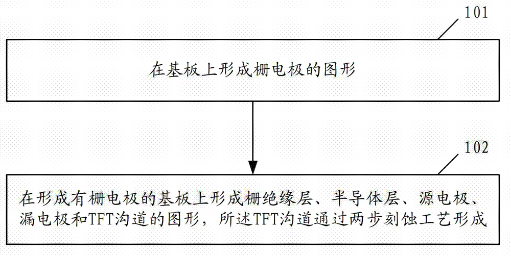
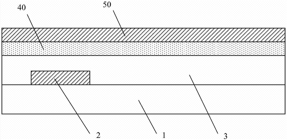
[0044]Aiming at the problem that in the prior art when manufacturing metal oxide thin film transistors, no matter whether dry etching or wet etching is used, the metal oxide under the TFT channel region may be converted into a conductor, thereby making the thin film transistor invalid. The embodiment of the invention provides a method for manufacturing a thin film transistor and a method for manufacturing an array substrate. The semiconductor layer of the thin film transistor is made of metal oxide. The manufacturing method uses two-step etching to form a TFT channel. The first step is through Dry etching removes part of the source and drain metal layer in the TFT channel region above the semiconductor layer without damaging the semiconductor layer b...


PUM


Abstract

The invention provides a method for manufacturing a thin film transistor (TFT), another method for manufacturing an array substrate and a display device, which belongs to the technical field of manufacturing of semiconductors. The semiconductor layer of the thin film transistor is formed by metal oxide. According to the method for manufacturing the thin film transistor, a TFT channel is formed by etching in two steps, first step, a part of a source drain metal layer in a channel area above the semiconductor layer is removed by dry etching; and second step, the rest source drain metal layer in the channel area above the semiconductor layer is removed by wet etching to form the TFT channel. According to the invention, the metal oxide semiconductor layer below the TFT channel can be protected without forming an etching barrier layer.

Description

technical field [0001] The invention relates to the technical field of semiconductor manufacturing, in particular to a manufacturing method of a thin film transistor, a manufacturing method of an array substrate and a display device. Background technique [0002] Due to its high mobility and good uniformity, metal oxide thin film transistors have attracted people's attention and have become a recent research hotspot. The manufacture of the array substrate with metal oxide thin film transistors can be completed by four patterning processes, which specifically include: forming the pattern of the gate electrode and the gate line on the substrate through the first patterning process; forming a gate insulating layer; The patterning process forms the pattern of the semiconductor layer, source electrode, drain electrode, data line and thin film transistor (TFT) channel on the gate insulating layer; the pattern of the passivation layer is formed through the third patterning process,...

Claims


Application Information

Patent Timeline
IPC IPC(8): H01L21/34H01L21/77
CPCH01L29/7869H01L27/1225H01L29/66969
Inventor 刘圣烈严允晟
Owner BOE TECH GRP CO LTD
Why Eureka
Try Eureka