Photomask blank, method for manufacturing photomask, and method for manufacturing phase shift mask

a technology of photomask and mask, which is applied in the field of photomask blank, can solve the problems of unwilling limitation of effect in view of shortening the total etching time, the inability to completely avoid the decrease in optical density, and the burden on the photoresist pattern or hard mask pattern at the time of transferring the pattern on the light-shielding film, etc., to achieve the effect of reducing the burden on the photoresist pattern or hard mask pattern at the tim

Active Publication Date: 2013-11-21
SHIN ETSU CHEM IND CO LTD
View PDF1 Cites 9 Cited by
  • Summary
  • Abstract
  • Description
  • Claims
  • Application Information

AI Technical Summary

Benefits of technology

[0038]In the present invention, a light-shielding film formed on a photomask blank is configured as one having a monolayer structure or a multilayer structure, at least one of the layers is a layer made of a chromium-containing material, and at least one of the layers made of a chromium-containing material is made of a chromium-containing material including tin. The layer made of a chromium-containing material including tin can cause a significant increase in the etching rate at the time of chlorine-containing dry etching including oxygen.
[0039]Thus, burden on the photoresist pattern or hard mask pattern at the time of transferring a pattern on the light-shielding film is reduced, and therefore it is possible to carry out pattern transfer with high precision. Therefore, since the pattern transfer to the light-shielding film results in high precision patterning, it becomes possible to manufacture a binary mask, a Levenson mask, or the like on which high-precision pattern is formed.

Problems solved by technology

However, the technique as described above, where a light element is added to a chromium-containing compound to suppress a decrease in thickness of a photoresist film by increasing the dry-etching rate of a light-shielding film, has the following disadvantage:
For example, a decrease in optical density cannot be completely avoided when the addition of a light element is carried out to enhance an etching rate.
Thus, an effect is unwillingly limited in view of shortening the total etching time.

Method used


Image

  • Photomask blank, method for manufacturing photomask, and method for manufacturing phase shift mask
  • Photomask blank, method for manufacturing photomask, and method for manufacturing phase shift mask
  • Photomask blank, method for manufacturing photomask, and method for manufacturing phase shift mask

Examples


example 1

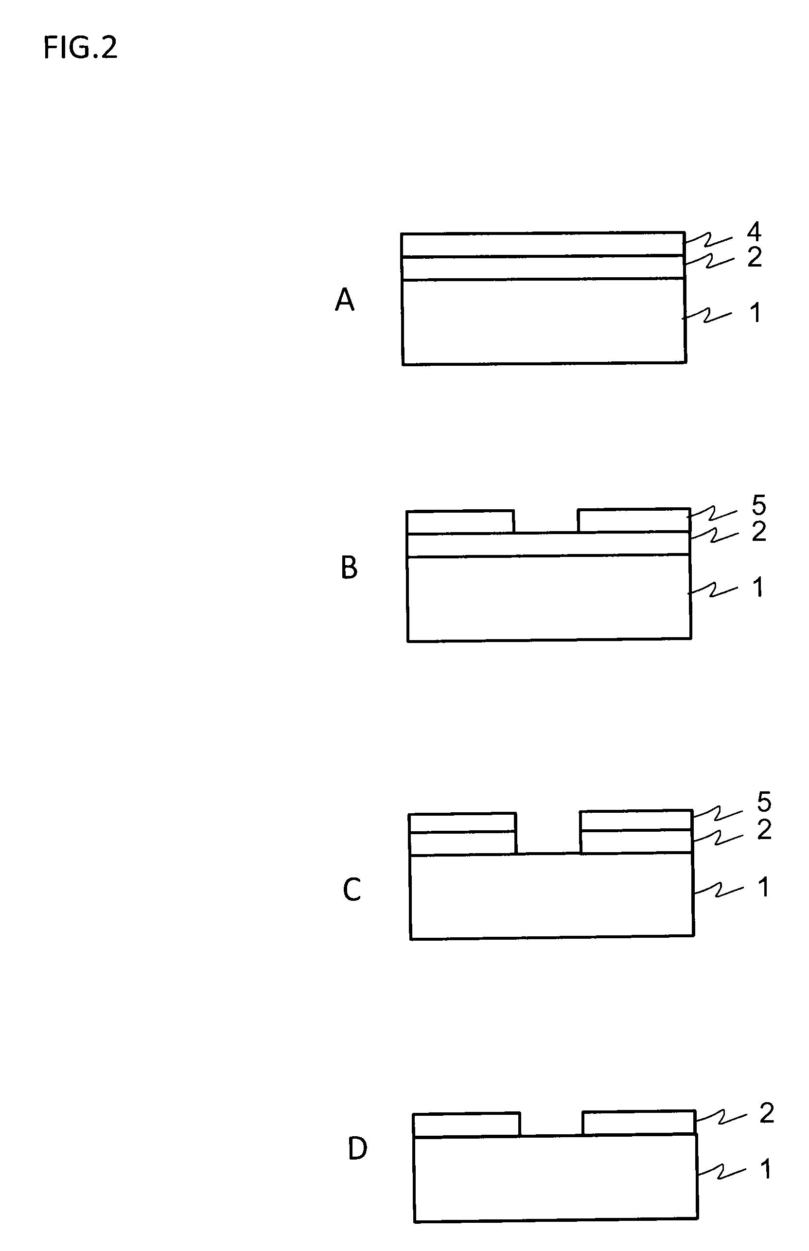
[0152]A light-shielding film including a light-shielding layer and an anti-reflection layer was formed on a quartz substrate by using a direct-current sputtering device. As a light-shielding layer, a film (46 nm in film thickness) made of chromium, tin, and nitrogen was formed on the quartz substrate.

[0153]Using two different targets, a chromium target and a tin target, as targets, film-formation was carried out on the quartz substrate in rotation at 30 rpm. Sputtering gas used was Ar and nitrogen and adjusted so that the inside of a gas chamber could have a gas pressure of 0.05 Pa.

[0154]When the composition of this light-shielding layer was investigated by ESCA, it was Cr:Sn:N=6:1:2 (atomic ratio).

[0155]On the light-shielding layer, film-formation of an anti-reflection layer (23 nm in film thickness) made of chromium, tin, nitrogen, and oxygen was carried out by using a direct-current sputtering device.

[0156]Using two different targets, a chromium target and a tin target, as target...

embodiment 2

[0162]A light-shielding film including a light-shielding layer and an anti-reflection layer was formed on a quartz substrate by using a direct-current sputtering device. As a light-shielding layer, a film (46 nm in film thickness) made of chromium, tin, and nitrogen was formed on the quartz substrate.

[0163]Using two different targets, a chromium target and a tin target, as targets, film-formation was carried out on the quartz substrate in rotation at 30 rpm. Sputtering gas used was Ar and nitrogen and adjusted so that the inside of a gas chamber could have a gas pressure of 0.05 Pa.

[0164]When the composition of this light-shielding layer was investigated by ESCA, it was Cr:Sn:N=6:1:2 (atomic ratio).

[0165]On the light-shielding layer, film-formation of an anti-reflection layer (23 nm in film thickness) made of chromium, tin, and nitrogen was carried out by using a direct-current sputtering device.

[0166]Using two different targets, a chromium target and a tin target, as targets, film-...

example 3

[0176]A light-shielding film including a light-shielding layer and an anti-reflection layer was formed on a quartz substrate by using a direct-current sputtering device. As a light-shielding layer, a film (46 nm in film thickness) made of chromium, tin, and nitrogen was formed on the quartz substrate.

[0177]Using two different targets, a chromium target and a tin target, as targets, film-formation was carried out on the quartz substrate in rotation at 30 rpm. Sputtering gas used was Ar and nitrogen and adjusted so that the inside of a gas chamber could have a gas pressure of 0.05 Pa.

[0178]When the composition of this light-shielding film was investigated by ESCA, it was Cr:Sn:N=6:1:2 (atomic ratio).

[0179]On the light-shielding layer, film-formation of an anti-reflection layer (23 nm in film thickness) made of chromium, tin, nitrogen, and oxygen was carried out by using a direct-current sputtering device.

[0180]Using two different targets, a chromium target and a tin target, as targets...


PUM

PropertyMeasurementUnit
optical densityaaaaaaaaaa

Abstract

A light-shielding film 2 formed on a transparent substrate 1 has a monolayer structure or a multilayer structure. At least one layer is formed by film-formation with a chromium-containing material including tin. The light-shielding film 2 has an optical density of 2 or higher and 4 or lower and has a reflection-preventing function. The layer made of a chromium-containing material including tin, which constitutes the light-shielding film 2, can cause a significant increase in the etching rate at the time of chlorine-containing dry etching including oxygen. Thus, burden on the resist pattern or hard mask pattern at the time of transferring a pattern on the light-shielding film is reduced, and therefore it is possible to carry out pattern transfer with high precision.

Description

TECHNICAL FIELD [0001]The present invention relates to a photomask blank for a photomask used in manufacture of a semiconductor integrated circuit or the like. More specifically, the present invention relates to a binary mask blank and a method for manufacturing a photomask using such a mask blank.BACKGROUND ART [0002]A microfabrication technique is a very important basic technique in the field of semiconductor technology, and the research and development thereof have been progressed for further finer microfabrication. In recent years, particularly, with high integration of a large scale integration circuit, refinement of circuit patterns, wiring patterns, or contact-hole patterns for wiring between layers forming a cell has been progressed, and a request for microfabrication technology has been increased.[0003]In connection with this, even in the field of technology for photomask production to be used in the process for photolithography in microfabrication, a technique for forming ...

Claims


Application Information

Patent Timeline
Patent Type & Authority Applications(United States)
IPC IPC(8): G03F1/26
CPCG03F1/30G03F1/26G03F1/80G03F1/54G03F1/20H01L21/0274
Inventor FUKAYA, SOUICHINAKAGAWA, HIDEOSASAMOTO, KOUHEI
Owner SHIN ETSU CHEM IND CO LTD
Why Eureka
Try Eureka