
Bottom antireflective coating compositions and processes thereof

Active Publication Date: 2012-12-06
MERCK PATENT GMBH
View PDF4 Cites 43 Cited by
  • Summary
  • Abstract
  • Description
  • Claims
  • Application Information

AI Technical Summary

Benefits of technology

[0006]The use of absorbing antireflective coatings in photolithography is a simpler approach to diminish the problems that result from back reflection of light from highly reflective substrates. The bottom antireflective coating is applied on the substrate and then a layer of photoresist is applied on top of the antireflective coating. The photoresist is exposed imagewise and developed. The antireflective coating in the exposed area is then typically etched and the photoresist pattern is thus transferred to the substrate. Most antireflective coatings known in the prior art are designed to be dry etched. The etch rate of the antireflective film needs to be relatively high in comparison to the photoresist so that the antireflective film is etched without excessive loss of the resist film during the etch process. There are two known types of antireflective coatings, inorganic coatings and organic coatings. These types of coatings have been designed for removal by dry etching.
[0007]In addition, photoresist patterns may be damaged or may not be transferred exactly to the substrate if the dry etch rate of the antireflective coating is similar to or less than the etch rate of the photoresist coated on top of the antireflective coating. The etching conditions for removing the organic coatings can also damage the substrate. Thus, there is a need for both organic bottom antireflective coatings that can be dry etched and organic bottom antireflective coatings that can be removed by the photoresist developer without dry etching, and can also provide good lithographic performance, especially for compound semiconductor type substrates, which are sensitive to etch damage.
[0008]The novel approach of the present application is to use an absorbing bottom antireflective coating film; especially a bottom antireflective coating that can be dry etched or developed by an aqueous alkaline developer solution. Aqueous removal of the bottom antireflective coating eliminates the dry etch rate requirement of the coating, reduces the cost intensive dry etching processing steps and also prevents damage to the substrate caused by dry etching. The novel bottom antireflective coating compositions of the present invention contain a novel additive, a crosslinking compound and a polymer.SUMMARY OF THE INVENTION

Problems solved by technology

Thus, treatment of an exposed positive-working photoresist with a developer causes removal of the exposed areas of the photoresist coating and the formation of a positive image in the coating, thereby uncovering a desired portion of the underlying substrate surface on which the photoresist composition was deposited.
In addition, photoresist patterns may be damaged or may not be transferred exactly to the substrate if the dry etch rate of the antireflective coating is similar to or less than the etch rate of the photoresist coated on top of the antireflective coating.
The etching conditions for removing the organic coatings can also damage the substrate.

Method used


Image

  • Bottom antireflective coating compositions and processes thereof
  • Bottom antireflective coating compositions and processes thereof
  • Bottom antireflective coating compositions and processes thereof

Examples


synthesis example 1

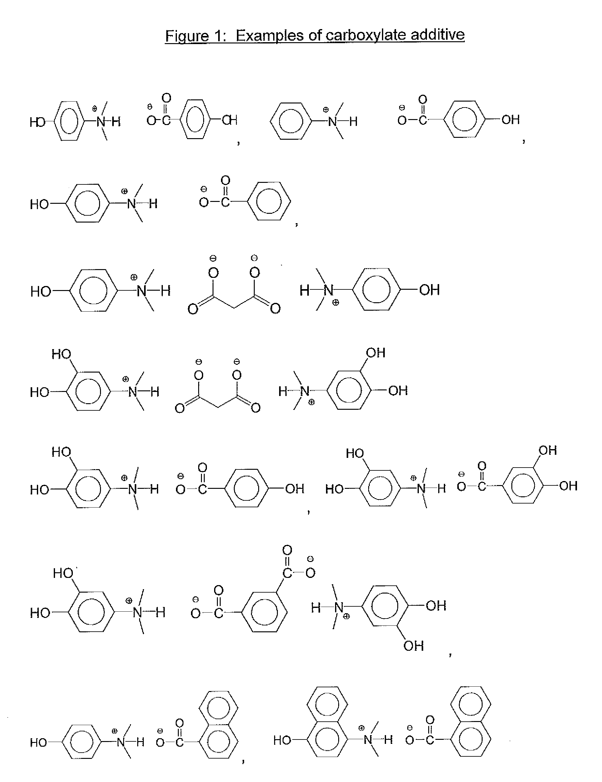
[0066]1.52 g of 4-hydroxyphenylacetic acid was dissolved in 40.37 g of propylene glycol mono methylether (PGME). To the above PGME solution, 2.96 g of trihexylamine was added and mixed.

[0067]The solution was heated at 40° C. under reduced pressure using a rotary evaporator and the product was isolated. H-NMR spectrum showed N+CH2 proton at 3.5 ppm. Proton of free carboxyl group was not observed and formation of carboxylic acid salt was confirmed.

synthesis examples 2-15

[0068]Table 1 lists examples 1-15 which were all the salts which were made as stock solutions in PGME and used in the formulation examples. These were reacted in the same manner as shown above, but leaving the materials in PGME as stock solutions to be used in the above described formulation examples.

TABLE 1Synth.ExCarboxylic acidAmineSolvent14-hydroxyphenyl aceticTrihexylamine (2.96 g)PGME (40.37 g)acid (1.52 g)24-hydroxyphenyl aceticTriethylamine (1.11 g)PGME (23.71 g)acid (1.52 g)34-hydroxyphenyl acetic3-(dimethylamino)phenol (1.51 g)PGME (27.27 g)acid (1.52 g)44-hydroxyphenyl acetic3-(diethylamino)phenol (1.82 g)PGME (30.05 g)acid (1.52 g)5Malonic acid (1.04 g)3-(dimethylamino)phenol (3.01 g)PGME (36.52 g)6Malonic acid (1.04 g)3-(diethylamino)phenol (3.64 g)PGME (42.08 g)74-(4-Trihexylamine (1.48 g)PGME (21.77 g)hydroxyphenyl)benzoicacid (1.07 g)82-(4-Trihexylamine (1.48 g)PGME (20.33 g)hydroxylphenoxy)propionicacid (0.91 g)94-hydroxybenzoic acidTrihexylamine (1.48 g)PGME (18.34...

example 1

Formulation and Exposure Example 1

[0069]PQMA / EAdMA (60 / 40) copolymer (0.2218 g), tris(vinyloxybutyl)cyclohexane 1,2,4-tricarboxylate (0.0665 g), triethylaminium 4-hydroxyphenylacetate (0.0670 g) and bis[tris(4-vinyloxyethoxyphenyl)sulfonium]perfluorobutanedisulfonate (0.0047 g) were dissolved in a mixture of 13.57 g of propyleneglycol monomethylether, 5.81 g of propyleneglycol monomethylether acetate and 0.241 g of γ-valerolactone to form a antireflective composition (B.A.R.C.) solution. The solution was filtered through a 0.2 μm micron filter.

[0070]The B.A.R.C. solution was coated on a silicon wafer and heated on a hotplate at 190° C. for 60 seconds to give a film thickness of 400 Å. The absorption (k) value was 0.38 and the refractive index (n) value was 1.726 at 193 nm. The B.A.R.C. wafer was prewet with a solvent and coated with 193 nm photoresist and heated on a hotplate for 110° C. for 60 seconds to give a film thickness of 140 nm. The coated wafer was exposed using Nikon 306D...


PUM

PropertyMeasurementUnit
Compositionaaaaaaaaaa
Structureaaaaaaaaaa
Antireflectiveaaaaaaaaaa

Abstract

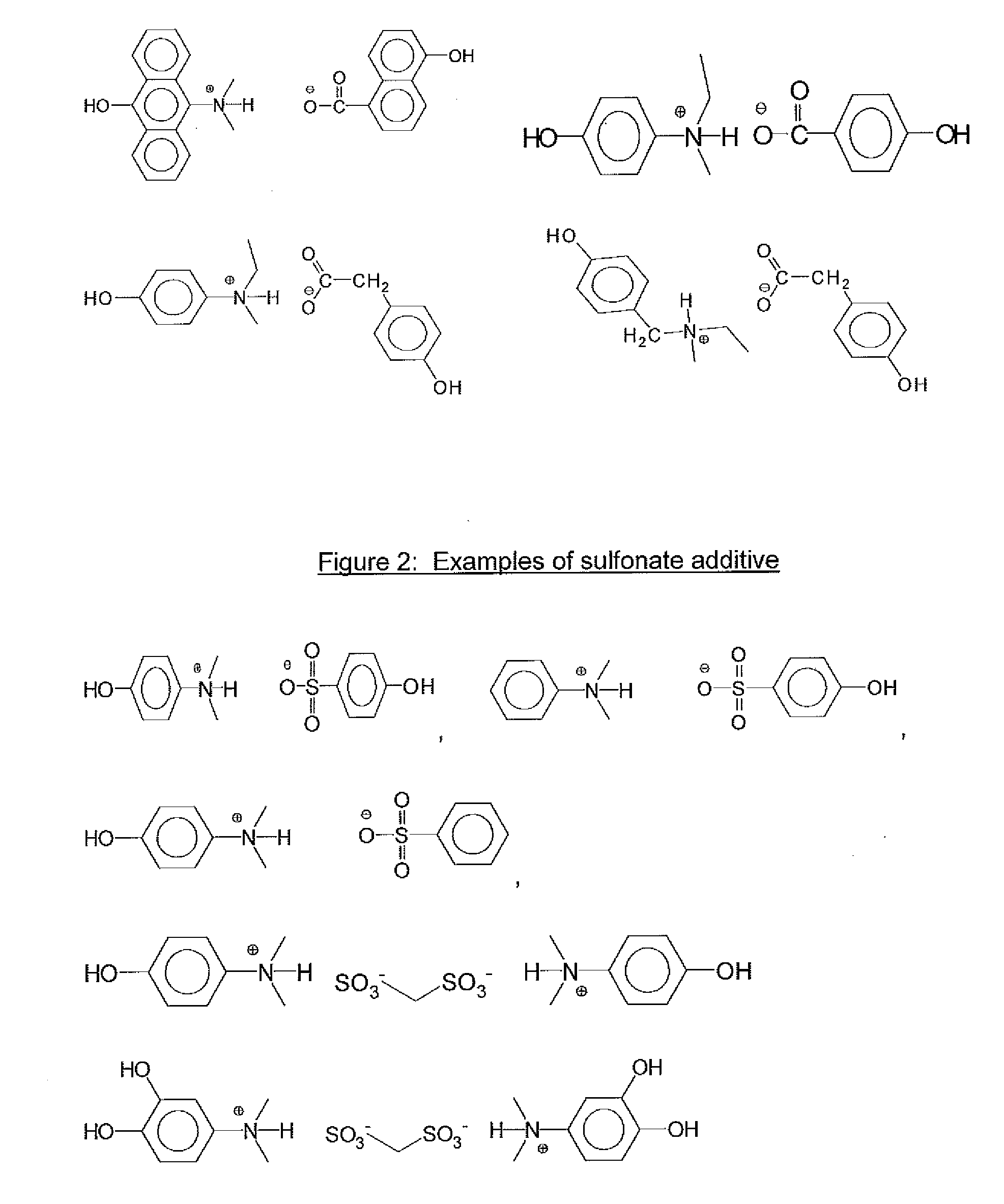
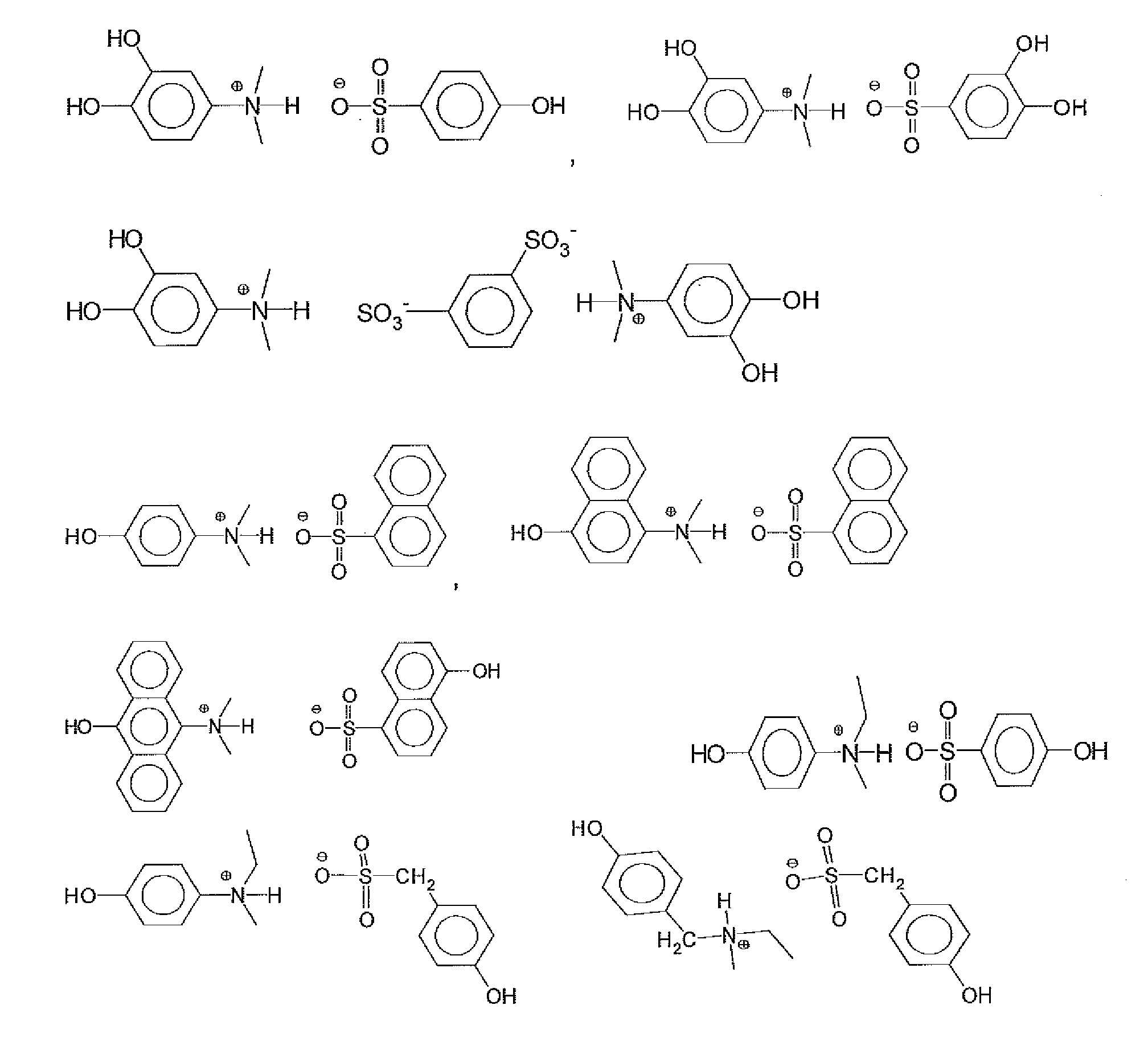
The present invention relates to an antireflective coating composition comprising a crosslinking agent, a polymer comprising at least one chromophore group and at least one hydroxyl and / or a carboxyl group, and an additive, further where the additive has structure 1 and comprises at least one arylene-hydroxyl moiety,where Y is selected from an carboxylate anion or sulfonate anion, R1, R2, and R3 are independently selected from unsubstituted C1-C8 alkyl, substituted C1-C8 alkyl, aryl and arylene-hydroxyl; X1, X2, and X3 are independently selected from direct valence bond and C1-C8 alkylene group, and, n=1, 2 or 3. The invention further relates to a process for using the composition.

Description

[0001]The present invention relates to novel antireflective coating compositions and their use in image processing by forming a thin layer of the novel antireflective coating composition between a reflective substrate and a photoresist coating. Such compositions are particularly useful in the fabrication of semiconductor devices by photolithographic techniques, especially those requiring exposure with deep ultraviolet radiation.[0002]Photoresist compositions are used in microlithography processes for making miniaturized electronic components such as in the fabrication of computer chips and integrated circuits. Generally, in these processes, a thin coating of a film of a photoresist composition is first applied to a substrate material, such as silicon wafers used for making integrated circuits. The coated substrate is then baked to evaporate any solvent in the photoresist composition and to fix the coating onto the substrate. The baked and coated surface of the substrate is next subj...

Claims


Application Information

Patent Timeline
IPC IPC(8): G03F7/20C08K5/42
CPCG03F7/091C09D5/006C09D5/00G02B1/11H01L21/027
Inventor KUDO, TAKANORIDIOSES, ALBERTONG, EDWARDCHAKRAPANI, SRINIVASANPADMANABAN, MUNIRATHNA
Owner MERCK PATENT GMBH
Learn More