Reflective mask blank for EUV lithography and process for producing the same

a technology of euv lithography and reflector, which is applied in the direction of photomechanical equipment, originals for photomechanical treatment, instruments, etc., can solve the problems of inability to use a conventional refractive optical system like photolithography, the conventional photolithography method is close to its limit the etching apparatus can be simplified, so as to reduce contamination during the etching process, the etching process is simplified, and the etching process is reduced

Active Publication Date: 2012-12-20
ASAHI GLASS CO LTD
View PDF3 Cites 51 Cited by
  • Summary
  • Abstract
  • Description
  • Claims
  • Application Information

AI Technical Summary

Benefits of technology

[0042]When the EUV mask blank of the present invention is used, a sufficient etching rate as compared with conventional low reflective layers may be obtained even in an etching process using a chlorine type gas. Thus, etching of a reflective layer and an absorber layer only by a chlorine type gas is possible, and it is expected that the etching process and the etching apparatus can be simplified, as well as it is expected that contamination during the etching process can be reduced. Further, according to the present invention, etching rate of the low reflective layer is higher than that of a conventional reflective layer, whereby it is possible to make a resist thinner than it already is, and as a result, it is expected that a finer patterning may become possible.
[0043]Further, in the EUV mask blank of the present invention, the low reflective layer has good adhesion with a resist, whereby it is possible to solve problems such that a resist pattern disappears or a resist pattern falls down and becomes a defect of the resist pattern when a fine resist pattern having a width of about 100 nm or less is formed.
[0044]Further, according to the process for producing an EUV mask blank of the present invention, an EUV mask blank excellent in various kinds of properties may easily be obtained, as described above.

Problems solved by technology

However, the conventional photolithography method has come close to its limit, while miniaturization of semiconductor devices is being accelerated.
EUV light is likely to be absorbed by all kinds of substances, and the refractive indices of substances at such a wavelength are close to 1, whereby it is not possible to use a conventional refractive optical system like photolithography employing visible light or ultraviolet light.
On the other hand, however, when a layer composed of an oxide or a layer composed of oxynitride is employed as the low reflective layer, there is a problem of a decrease in etching rate as described below.
However, when such a two-step etching process is carried out, two etching chambers are required, and thus the process becomes complicated and there is concern about contamination during transfer between chambers.
Further, in a case where two steps of the etching process are carried out in a chamber, different types of gases i.e. a fluorine type gas and a chlorine type gas are mixed, and thus problems may occur such as contamination of the chamber and destabilization of the process.
However, the EUV mask blank disclosed in Patent Document 4 has a low reflective layer which is a film containing Si, and thus there is a concern that a problem about adhesion with a resist for a mask pattern as described in paragraph of Patent Document 5 may occur.
That is, in the case where the low reflective layer is a Si-containing film, the adhesion with a resist which is applied at the time of forming a mask pattern is insufficient, and when a fine resist pattern is formed, specifically, when a fine resist pattern having a width of about 100 nm or less, problems may occur such that a resist pattern disappears or a resist pattern falls down and becomes a defect of the resist pattern.

Method used


Image

  • Reflective mask blank for EUV lithography and process for producing the same
  • Reflective mask blank for EUV lithography and process for producing the same

Examples


example 1

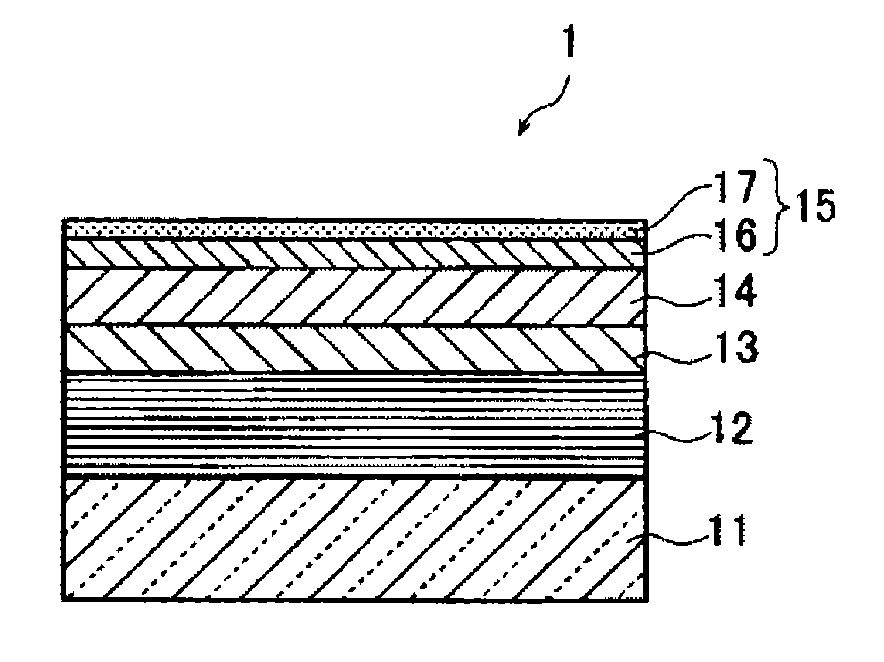
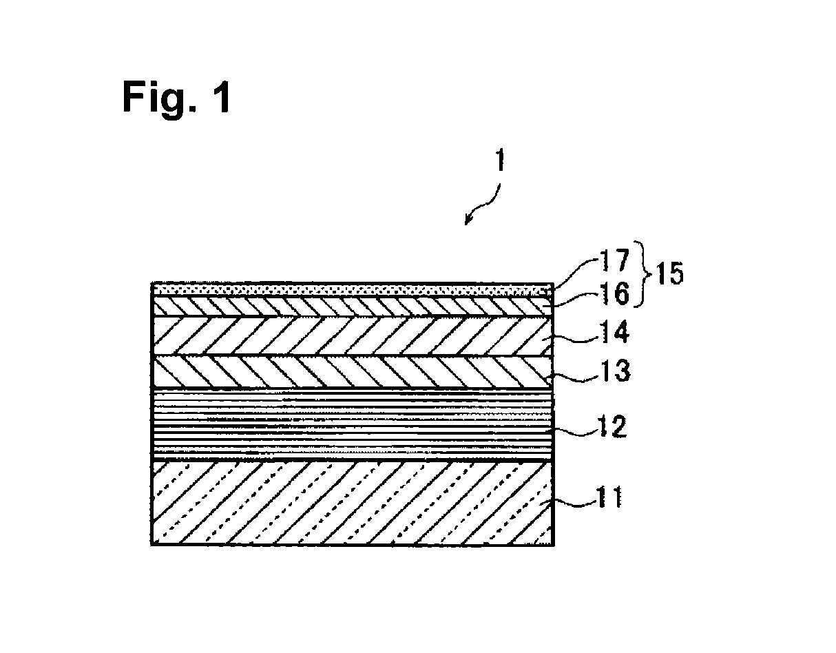
[0160]In this Example, an EUV mask blank 1 as shown in FIG. 1 was prepared.

[0161]As a substrate 11 for film formation, a SiO2—TiO2 type glass substrate (shape: about 6 inch square (length×width: about 152 mm×about 152 mm), thickness: about 6.3 mm) was used. This glass substrate has a thermal expansion coefficient of 0.2×10⁻⁷ / ° C., a Young's modulus of 67 GPa, a Poisson's ratio of 0.17 and a specific rigidity of 3.07×10⁷ m2 / s2. This glass substrate was polished to form a smooth surface having a surface roughness (rms) of at most 0.15 nm with a planarity of at most 100 nm.

[0162]On the rear surface side of the substrate 11, a Cr film having a thickness of 100 nm was formed by a magnetron sputtering method to provide a high dielectric coating having a sheet resistance of 100 Ω / □.

[0163]By using the formed Cr film, the substrate 11 was fixed to a usual electrostatic chuck of a flat plate shape, and on the surface of the substrate 11, a Si film and a Mo film were alternately formed by mean...

example 2

[0223]In this Example, film formation and evaluation were carried out in the same manner as in Example 1 except that a TaON film having a thickness of 3 nm was formed as the second layer 17, and the etching time was changed as shown in Table 3. Consequently, results shown in Tables 1, 2 and 4 were obtained.

example 3

[0224]In this Example, film formation and evaluation were carried out in the same manner as in Example 1 except that as the second layer 17, a TaN film having a thickness of 1 nm were formed under the same condition as the absorber layer 14, and the etching time was changed as shown in Table 3. Consequently, results shown in Tables 1, 2 and 4 were obtained.

[0225]Such obtained TaN film had a Ta content of 57 at % and a N content of 43 at %.


PUM

PropertyMeasurementUnit
wavelengthaaaaaaaaaa
surface roughnessaaaaaaaaaa
total thicknessaaaaaaaaaa

Abstract

To provide an EUV mask blank provided with a low reflective layer, which has excellent properties as an EUV mask blank. A reflective mask blank for EUV lithography comprising a substrate, and a reflective layer for reflecting EUV light, an absorber layer for absorbing EUV light and a low reflective layer to an inspection light (wavelength: 190 to 260 nm) for a mask pattern, formed in this order on the substrate, wherein the low reflective layer has a stacked structure having a first layer containing at least 95 at % in total of silicon (Si) and nitrogen (N), and a second layer containing at least 95 at % in total of tantalum (Ta), oxygen (O) and nitrogen (N) or a second layer containing at least 95 at % in total of tantalum (Ta) and nitrogen (N), stacked in this order from the absorber layer side.

Description

TECHNICAL FIELD[0001]The present invention relates to a reflective mask blank for EUV (Extreme Ultra Violet) lithography (in this specification, hereinafter referred to also as an “EUV mask blank”) to be used for e.g. production of semiconductors, a process for producing such a blank, a reflective mask for EUV lithography obtained by patterning the blank, and a process for producing a semiconductor integrated circuit by means of the reflective mask.BACKGROUND ART[0002]Heretofore, in the semiconductor industry, a photolithography method employing visible light or ultraviolet light has been used as a technique to transfer a fine pattern required to form an integrated circuit of a fine pattern on e.g. a Si substrate. However, the conventional photolithography method has come close to its limit, while miniaturization of semiconductor devices is being accelerated. In the case of the photolithography method, the resolution limit of a pattern is about ½ of the exposure wavelength. Even if ...

Claims


Application Information

Patent Timeline
Patent Type & Authority Applications(United States)
IPC IPC(8): G03F1/24G03F7/20G03F1/38G03F1/84
CPCG03F1/24G03F1/38G03F1/84G03F7/20G03F1/46C23C14/0036
Inventor UNO, TOSHIYUKIHAYASHI, KAZUYUKI
Owner ASAHI GLASS CO LTD
Why Eureka
Try Eureka