Dry etching method, production method for semiconductor element, and cleaning method

a production method and technology for semiconductor elements, applied in the direction of cleaning of hollow articles, surface treatment compositions, chemistry apparatus and processes, etc., can solve the problems of loss of semiconductor element characteristics, heavy load on the manufacturing apparatus of semiconductor elements, and difficult-to-etch materials containing metals, etc., to achieve sufficient etching rate

Pending Publication Date: 2022-07-21
RESONAC CORP
View PDF4 Cites 0 Cited by
  • Summary
  • Abstract
  • Description
  • Claims
  • Application Information

AI Technical Summary

Benefits of technology

[0029]According to the present invention, an etching object containing at least one metal element selected from among titanium, indium, and tin can be selectively etched at a sufficient etching rate without using plasma.

Problems solved by technology

To use materials containing the metals as semiconductor element materials, a technology for microfabricating the materials containing the metals into desired shapes is required, whereas many of the materials containing the metals are difficult-to-etch materials having almost no vapor pressure.
However, there has been a risk in that, if the wet etching method is adopted for the process of etching a semiconductor element, even a portion of the semiconductor element that should not be etched is inconveniently etched, resulting in loss of the characteristics of the semiconductor element.
However, the method disclosed in PTL 2 has been presenting a problem in that producing the halogen fluoride requires a high temperature, resulting in a heavy load on the semiconductor element manufacturing apparatus.
Further, the etching gas is a mixed gas of halogen fluoride and an unreacted halogen simple substance gas, so that there has been a risk in that a sufficient etching rate cannot be obtained.

Method used


Image

  • Dry etching method, production method for semiconductor element, and cleaning method
  • Dry etching method, production method for semiconductor element, and cleaning method

Examples


example 1-1

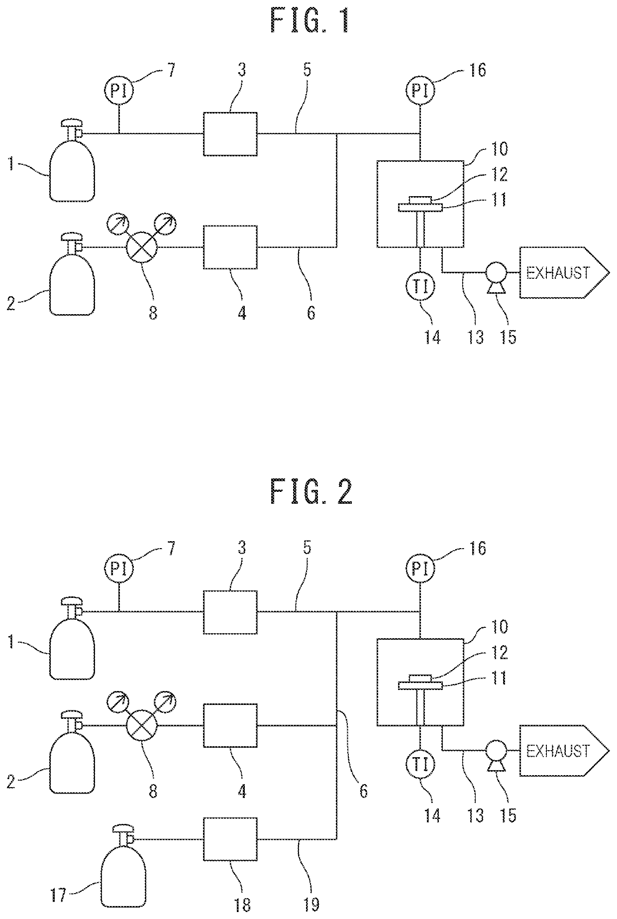
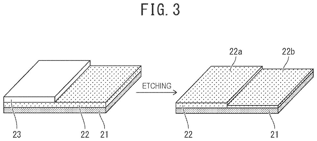
[0093]An etching object was etched by using an etching apparatus having substantially the same configuration as that of the etching apparatus of FIG. 1. A test piece (a member to be etched) used in Example 1-1 will be described with reference to FIG. 3.

[0094]A square silicon substrate 21 of 2 inches per side having a titanium oxide (TiO2) film 22 with a film thickness of 517 nm deposited thereon (manufactured by KST World Corporation) was prepared, and a rectangular nickel substrate 23 with dimensions of 1 inch×2 inches was bonded onto the titanium oxide film 22 by using grease (Demnum Grease L-200 manufactured by Daikin Industries, Ltd.) to create the test piece. The nickel substrate 23 was bonded so as to cover substantially half of the titanium oxide film 22 as illustrated in FIG. 3.

[0095]The test piece was placed on a stage inside a chamber of the etching apparatus, and the temperature of the stage was increased to 150° C. Subsequently, a bromine pentafluoride gas of a flow rate...

example 1-2

[0102]A test piece was etched in the same manner as in Example 1-1 except that iodine heptafluoride was used as the halogen fluoride, and a mixed gas formed by mixing an iodine heptafluoride gas of a flow rate of 50 mL / min and argon of a flow rate of 450 mL / min was used as the etching gas, and then the etching rate of the titanium oxide was calculated. The result is shown in Table 1.

example 1-3

[0103]A test piece was etched in the same manner as in Example 1-1 except that the temperature of the stage was set to 50° C., and then the etching rate of the titanium oxide was calculated. The result is shown in Table 1.


PUM

PropertyMeasurementUnit
temperatureaaaaaaaaaa
pressureaaaaaaaaaa

Abstract

A dry etching method which includes a dry etching step in which an etching gas containing a halogen fluoride, which is a compound of bromine or iodine and fluorine, is brought into contact with a member to be etched (12) having an etching object, which is an object to be etched by the etching gas, thereby etching the etching object without using plasma. The etching object contains at least one metal selected from among titanium, indium, and tin. Also disclosed is a production method for manufacturing a semiconductor element using the dry etching method as well as a cleaning method for cleaning an inner surface of a chamber of a semiconductor element manufacturing apparatus using the dry etching method.

Description

TECHNICAL FIELD[0001]The present invention relates to a dry etching method, a production method for a semiconductor element, and a cleaning method.BACKGROUND ART[0002]Materials containing metals such as titanium (Ti), indium (In), and tin (Sn) are used as hard masks or electrode materials for semiconductor elements in some cases. To use materials containing the metals as semiconductor element materials, a technology for microfabricating the materials containing the metals into desired shapes is required, whereas many of the materials containing the metals are difficult-to-etch materials having almost no vapor pressure.[0003]Therefore, microfabrication by a wet etching method, in which the materials containing the metals are removed by bringing a solution containing an oxidant, a chelating agent, a fluoride ion, or the like into contact with the materials containing the metals, has conventionally been a mainstream method (refer to, for example, PTL 1).[0004]However, there has been a ...

Claims


Application Information

Patent Timeline
Patent Type & Authority Applications(United States)
IPC IPC(8): H01L21/311H01L21/3213B08B9/08
CPCH01L21/31122H01L21/32135B08B2209/08H01L21/31144H01L21/32139B08B9/08H01L21/30604H01L21/3081H01L21/67069H01L21/67017C23F1/12H01L31/1888H01L21/302H01L21/3065C09K13/08
Inventor MATSUI, KAZUMA
Owner RESONAC CORP
Why Eureka
Try Eureka