Method for etching an object to be processed

a processing method and etching technology, applied in the direction of basic electric elements, electrical equipment, electric discharge tubes, etc., can solve the problems of insufficient etching selectivity of organic si-based low dielectric constant films, and none of the techniques yield satisfactory results

Inactive Publication Date: 2007-05-17
TOKYO ELECTRON LTD
View PDF20 Cites 1 Cited by
  • Summary
  • Abstract
  • Description
  • Claims
  • Application Information

AI Technical Summary

Benefits of technology

[0006] It is, therefore, a primary object of the present invention to provide an etching method capable of etching a SiC portion of an object to be processed with a sufficient etching rate.

Problems solved by technology

However, none of the techniques yield a satisfactory result due to providing a low etching rate of approximately 10 nm / min.
In addition to the low etching rate when etching the SiC film by using an organic Si-based low dielectric constant film formed thereon as a mask, the techniques fail to provide a sufficiently satisfactory etching selectivity with respect to the organic Si-based low dielectric constant film.

Method used


Image

  • Method for etching an object to be processed
  • Method for etching an object to be processed
  • Method for etching an object to be processed

Examples


Embodiment Construction

[0030] The preferred embodiments of the present invention will be described in detail with reference to the accompanying drawings.

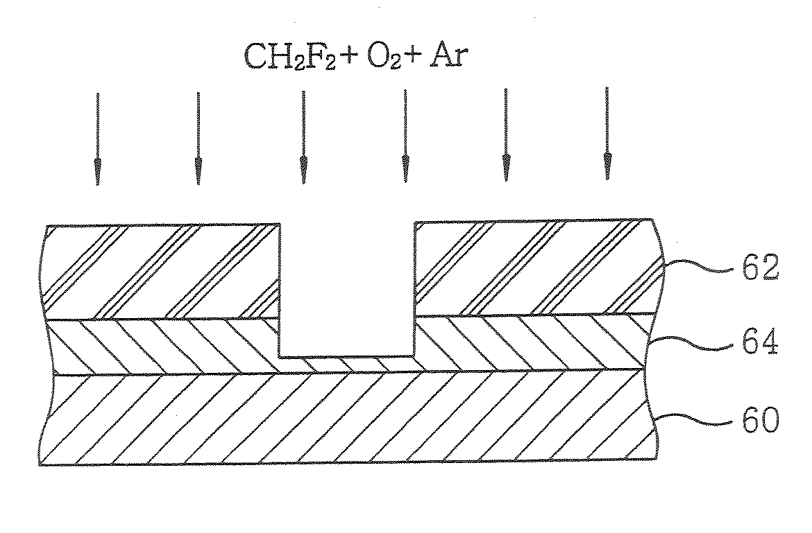
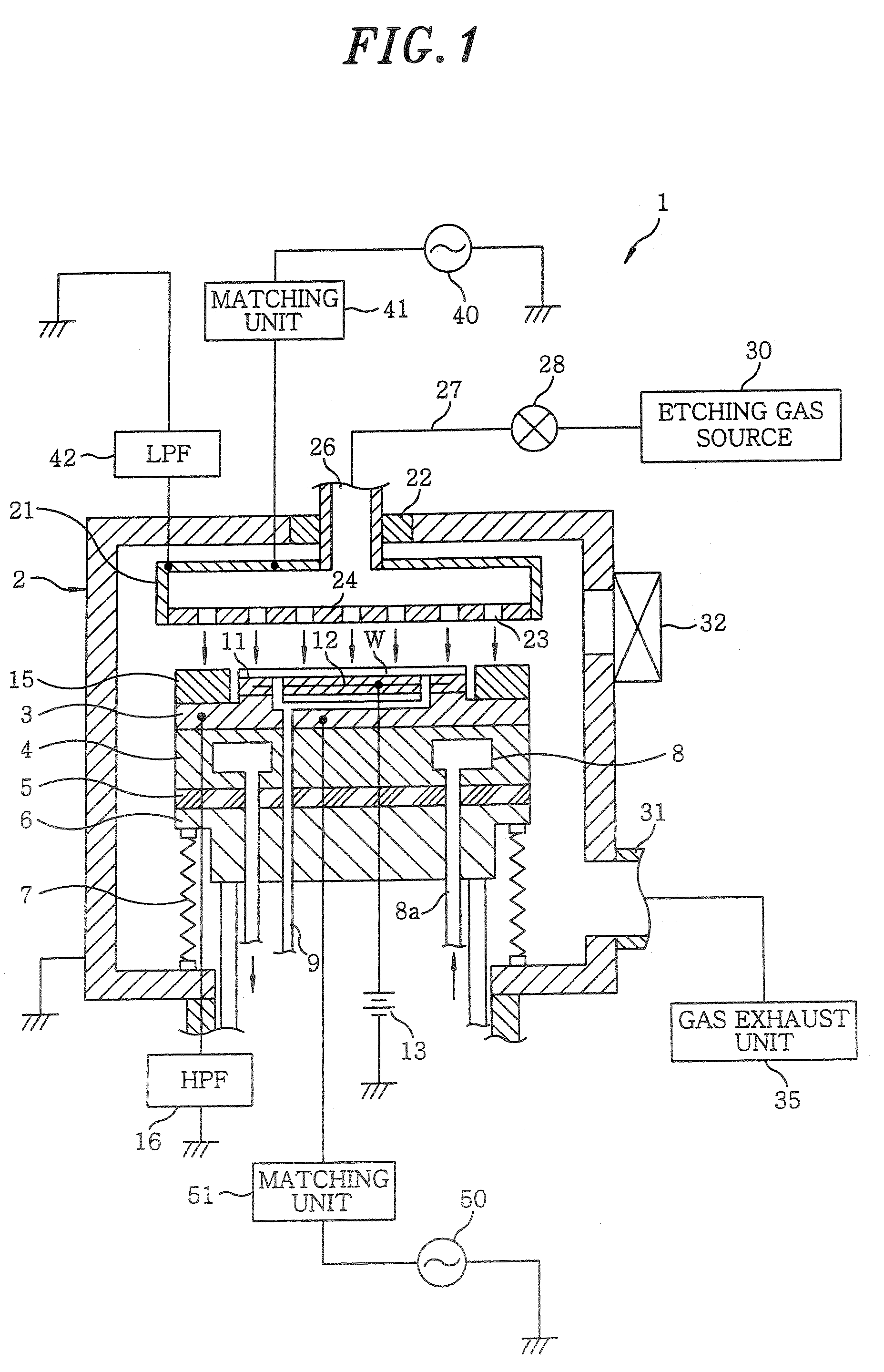
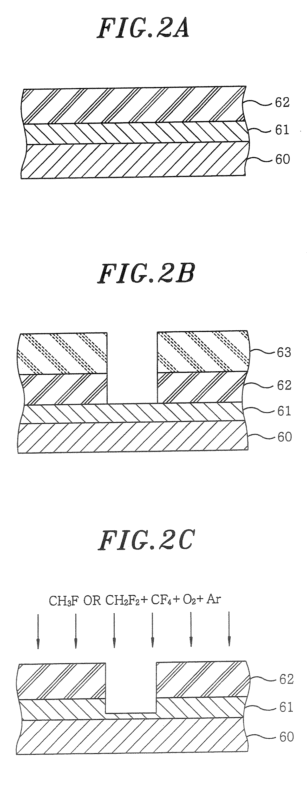
[0031]FIG. 1 is a schematic cross sectional view of a dry-etching apparatus for executing an etching method in accordance with a preferred embodiment of the present invention.

[0032] An etching apparatus 1 is a capacitively coupled parallel plate type etching apparatus having an upper and a lower electrode plates facing each other in parallel, wherein a high frequency power supply for generating a plasma is connected with one of the plates.

[0033] The etching apparatus 1 includes a chamber 2 of a cylindrical shape having a surface made of, e.g., aluminum treated with a thermal spray coating of ceramic, wherein the chamber 2 is frame-grounded. A susceptor 3 serving as a lower electrode is supported in the chamber 2 by a supporting member 4, for horizontally mounting thereon a semiconductor wafer (hereinafter referred to as a wafer) W made of, e.g., silico...


PUM


Abstract

An object to be process has a structure having an SiC film 61 and an organic Si-low dielectric constant film 62 formed on the SiC film 61. The SiC film 61 is etched using a plasma produced from an etching gas and using the organic Si low-dielectric constant film 62 as a mask. The etching gas contains CH2F2 or CH3F.

Description

FIELD OF THE INVENTION [0001] The present invention relates to a method for etching an object to be processed including an SiC or an SiN portion; and, more particularly, to a method for etching the SiC or the SiN portion of the object to be processed in a processing chamber by using a plasma of an etching gas, wherein the object may be, e.g., a semiconductor wafer having an SiC or an SiN film serving as a barrier layer and an interlayer insulating film formed thereon. BACKGROUND OF THE INVENTION [0002] In a wiring process of a semiconductor device, an interlayer insulating film formed between wiring layers is etched so that the wiring layers can be electrically connected with each other. In such a case, formed beneath the interlayer insulating film is an SiC or an SiN film serving as a barrier layer. When the SiC or the SiN film is etched to form a wiring pattern following an etching of the interlayer insulating film, the interlayer insulating film is used as a mask. [0003] Meanwhil...

Claims


Application Information

Patent Timeline
Patent Type & Authority Applications(United States)
IPC IPC(8): H01L21/82H01L21/302H01L21/027H01L21/3065H01L21/311H01L21/312H01L21/768
CPCH01J37/32082H01L21/0271H01L21/76802H01L21/31144H01L21/31116
Inventor FUSE, TAKASHIFUJIMOTO, KIWAMUYAMAGUCHI, TOMOYO
Owner TOKYO ELECTRON LTD
Why Eureka
Try Eureka