High efficiency solar cell fabrication

a solar cell and high-efficiency technology, applied in the direction of coatings, basic electric elements, solid-state devices, etc., can solve the problems of complex manufacturing processes currently formulated for such devices, and achieve the effects of reducing droplet size, improving etching rate, and improving positional control over deposition process

Inactive Publication Date: 2009-01-08
NEWSOUTH INNOVATIONS PTY LTD
View PDF14 Cites 46 Cited by
  • Summary
  • Abstract
  • Description
  • Claims
  • Application Information

AI Technical Summary

Benefits of technology

[0037]In the case where a small hole is required to be etched, this can be achieved by Inkjet printing a diluted etchant onto a hydrophobic surface layer and using subsequent evaporation of the etchant to reduce the droplet size while simultaneously increasing the etch rate so as to produce a hole through the surface layer of smaller diameter than the original droplet.
[0038]Alternatively a hydrophobic surface coating may be applied to the semiconductor structure prior to depositing the processing agent, whereby the processing agent when deposited forms tight droplets which do not spread out on the surface thereby providing better positional control over the deposition process.

Problems solved by technology

This has been achieved to some extent in thin film devices by use of large area devices carrying small quantities of silicon, however the manufacturing processes currently formulated for such devices are still complex and lend them selves to farther simplification or streamlining by finding new techniques.
However a challenge in such a device structure is achieving electrical isolation between the n and p regions, particularly when the respective regions are heavily doped (i.e. n+ and p+) to facilitate low resistance contacts.

Method used


Image

  • High efficiency solar cell fabrication
  • High efficiency solar cell fabrication
  • High efficiency solar cell fabrication

Examples


Embodiment Construction

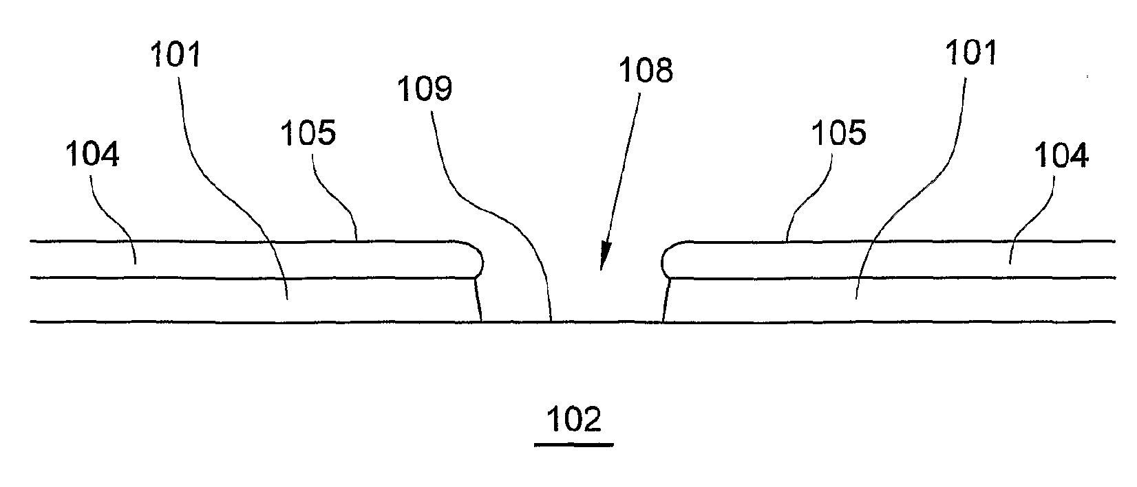
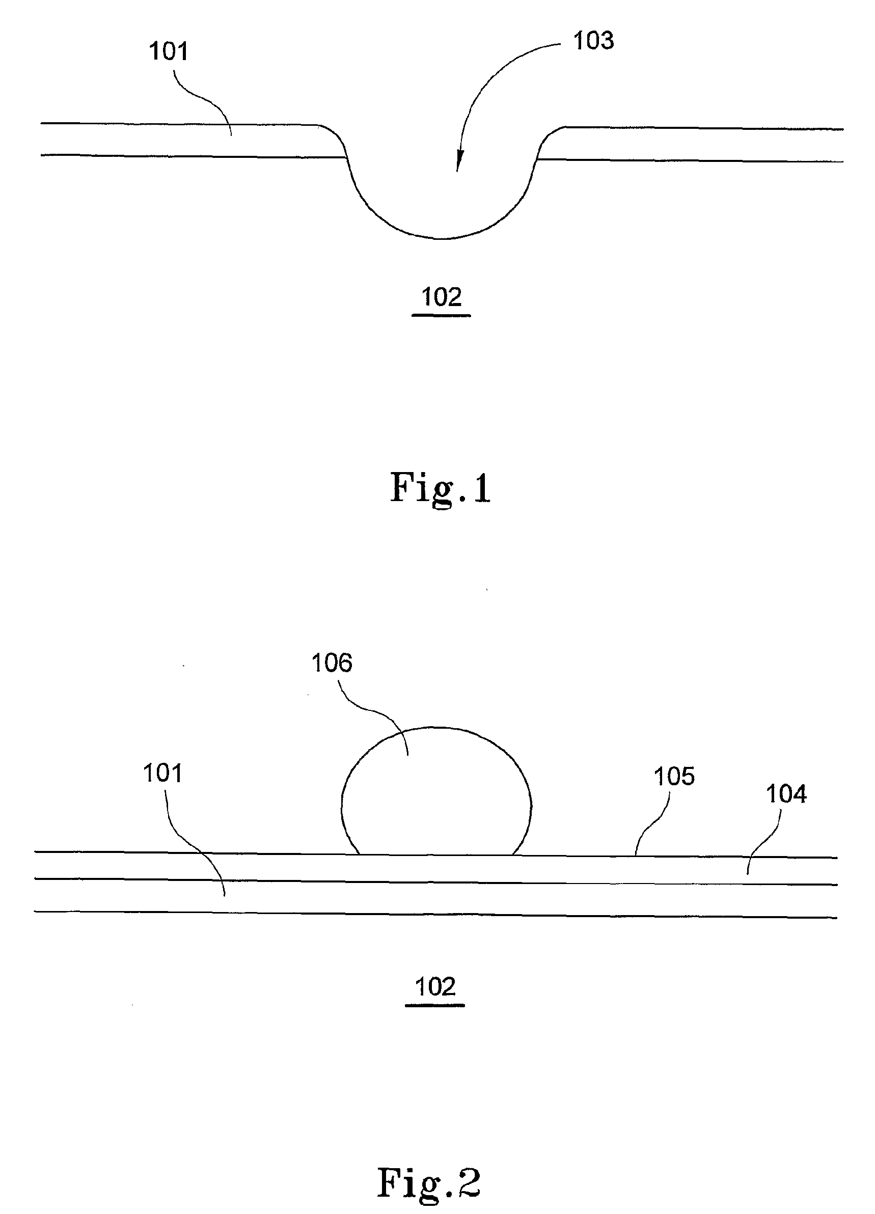
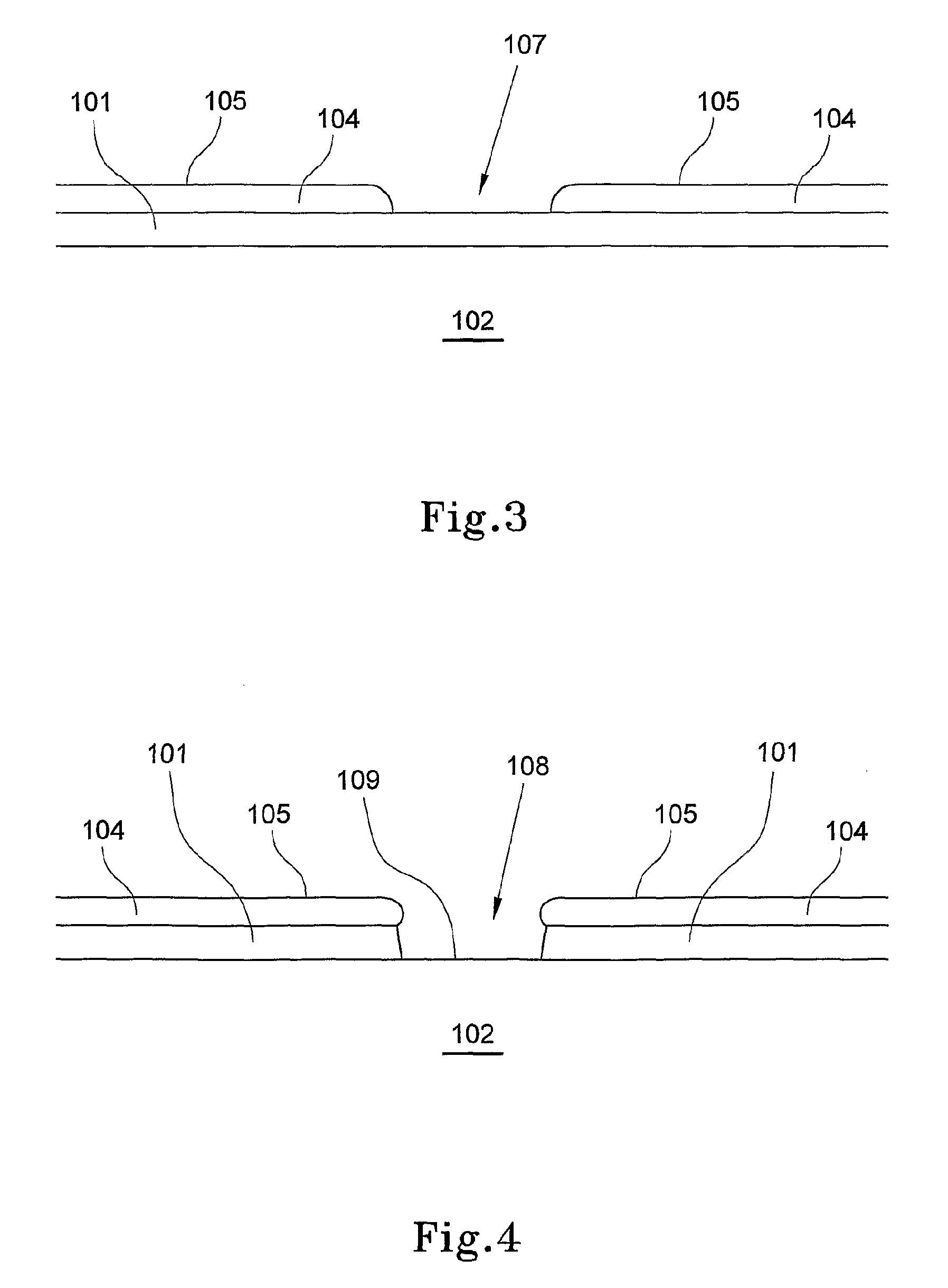
[0130]A new approach is described herein for enabling a metal contact to be applied to a layer or region of semiconductor material buried beneath another layer or region of semiconductor material doped with the opposite polarity. When making contact to the buried layer, achieving electrical isolation from the overlying semiconductor material of opposite polarity is of great importance, particularly in a photovoltaic device. An extension of this approach to contacting buried layers is the formation of metal contacts of both polarities from the same side of a device, while simultaneously providing excellent electrical isolation between the two polarities. This approach to forming contacts to buried layers also makes possible the formation of both polarities of metal contact with a single metal deposition process and it also makes it possible to form contacts to silicon material with a wide range of possible doping concentrations down to values below 1×10¹⁶ atoms / cm3.

[0131]This method ...


PUM


Abstract

A method of forming a contact structure and a contact structure so formed is described. The structure contacts an underlying layer of a semiconductor junction, wherein the junction comprises the underlying layer of a semiconductor material and is separated from an overlying layer of semiconductor material by creating an undercut region to shade subsequent metal formation. Various steps are performed using inkjet printing techniques.

Description

[0001]This invention relates generally to the field of solar cell fabrication and in particular it provides processing techniques making use of inkjet printing techniques to apply processing agents to the surface of a device under fabrication.BACKGROUND[0002]In order to make solar power a viable alternative to established generating methods such as fossil fuel and nuclear power, it is necessary to bring the manufacturing cost of solar cells down. This has been achieved to some extent in thin film devices by use of large area devices carrying small quantities of silicon, however the manufacturing processes currently formulated for such devices are still complex and lend them selves to farther simplification or streamlining by finding new techniques.[0003]In general, photovoltaic devices have two metal contacts, one of each polarity. In conventional structures one of these metal contacts, usually in a grid formation so as not to shade the semiconductor from too much light, is located ...

Claims


Application Information

Patent Timeline
Patent Type & Authority Applications(United States)
IPC IPC(8): H01L23/52H01L21/44H01L21/311B05C11/00
CPCH01L21/743Y02E10/50H01L31/022433H01L31/022425H01L31/04H01L31/18H01L21/44
Inventor WENHAM, STUART ROSSMAI, LYKUEPPER, NICOLE BIANCATJAHJONO, BUDI
Owner NEWSOUTH INNOVATIONS PTY LTD
Why Eureka
Try Eureka