Piezoelectric device and method for manufacturing piezoelectric device

a piezoelectric device and piezoelectric substrate technology, applied in the direction of piezoelectric/electrostrictive device details, device details, generators/motors, etc., can solve the problem of extremely low piezoelectric substrate etching rate in the +y axis direction, poor stress migration resistance, etc., to improve the power durability of the electrode and reduce the concentration of etching or etching time

Active Publication Date: 2014-07-10
MURATA MFG CO LTD
View PDF2 Cites 9 Cited by
  • Summary
  • Abstract
  • Description
  • Claims
  • Application Information

AI Technical Summary

Benefits of technology

[0032]Accordingly, various preferred embodiments of the present invention improves the power durability of an electrode formed on a piezoelectric thin film and a significant reduction in etchant concentration or etching time.

Problems solved by technology

Al electrodes, however, have poor stress migration resistance; a high electric power supplied to Al electrodes causes a hillock or void in the Al electrodes and finally shorts or breaks the Al electrodes, thus damaging the piezoelectric device.
The method in Japanese Unexamined Patent Application Publication No. 2002-305425 above, however, has the problem of an extremely low etching rate in the +Y axis direction of the piezoelectric substrate 2.
Increasing the etchant concentration or the etching time, however, causes a problem in that the bonding material 8 between the piezoelectric thin film 4 and the support substrate 9 dissolves in the strong acid.

Method used


Image

  • Piezoelectric device and method for manufacturing piezoelectric device
  • Piezoelectric device and method for manufacturing piezoelectric device
  • Piezoelectric device and method for manufacturing piezoelectric device

Examples


Embodiment Construction

[0046]A method for manufacturing a piezoelectric device according to a first preferred embodiment of the present invention will now be described with reference to FIGS. 3 to 7. As the method for manufacturing a piezoelectric device, a method for manufacturing a surface acoustic wave device will be described below by way of example.

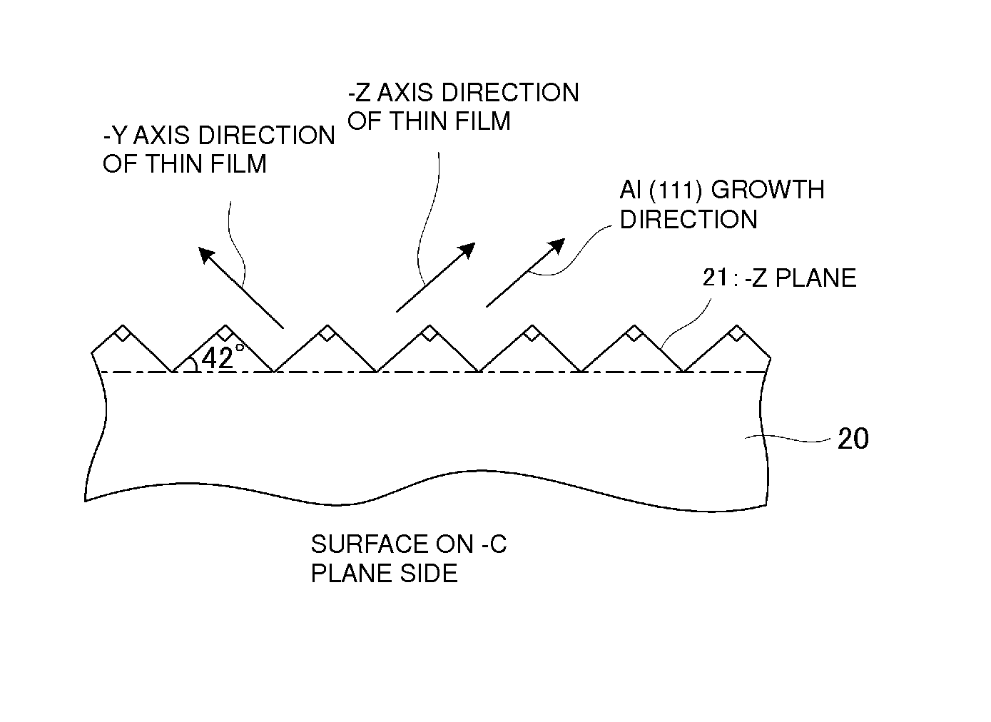
[0047]FIG. 3 is a flowchart showing the method for manufacturing a piezoelectric device according to the first preferred embodiment. FIGS. 4A-4C, 5A-5D, and 7A-7C are sectional views schematically showing the process for manufacturing a piezoelectric device shown in FIG. 3. FIG. 6A is a sectional view schematically showing a stepped structure on the −C plane side of a piezoelectric thin film 20 exposed after the completion of an etching step shown at S109 in FIG. 3. FIG. 6B is a sectional view schematically showing electrodes 60A to 60C epitaxially grown on −Z planes of the piezoelectric thin film 20 by an electrode-forming step shown at S110 in FIG. 3.

[00...


PUM

PropertyMeasurementUnit
cut angleaaaaaaaaaa
cut angleaaaaaaaaaa
cut angleaaaaaaaaaa

Abstract

In a method of manufacturing a piezoelectric device, among a +C plane on a +Z axis side of a piezoelectric thin film and a −C plane on a −Z axis side of the piezoelectric thin film, the −C plane on the −Z axis side of the piezoelectric thin film is etched. Thus, −Z planes of the piezoelectric thin film on which epitaxial growth is possible are exposed. Ti is epitaxially grown on the −Z planes of the piezoelectric thin film in the −Z axis direction such that the crystal growth plane thereof is parallel to the −Z planes of the piezoelectric thin film. Al is then epitaxially grown on the surface of the Ti electrode in the −Z axis direction such that the crystal growth plane thereof is parallel to the −Z planes of the piezoelectric thin film.

Description

BACKGROUND OF THE INVENTION[0001]1. Field of the Invention[0002]The present invention relates to piezoelectric devices including a piezoelectric thin film and methods for manufacturing such piezoelectric devices.[0003]2. Description of the Related Art[0004]Piezoelectric devices including a piezoelectric thin film are currently being developed. A plurality of methods for manufacturing a piezoelectric thin film are available to form such piezoelectric devices. For example, as disclosed in Japanese Unexamined Patent Application Publication No. 2002-534886, a method for manufacturing a piezoelectric device is developed in which a piezoelectric thin film is split off from a piezoelectric substrate along an ion-implanted layer.[0005]The method for manufacturing a piezoelectric device in which a piezoelectric thin film is split off from a piezoelectric substrate along an ion-implanted layer will now be described.[0006]FIG. 1 is a series of sectional views schematically showing a process fo...

Claims


Application Information

Patent Timeline
Patent Type & Authority Applications(United States)
IPC IPC(8): H01L41/04H01L41/187H01L41/297H01L41/047
CPCH01L41/04H01L41/297H01L41/1873H01L41/0477H03H3/08H03H9/14538H03H9/02929H03H9/02574H01L2224/11H10N30/8542H10N30/06H10N30/073Y10T29/42Y10T29/49005H10N30/067H10N30/80H10N30/877
Inventor ITO, KOREKIYOIWAMOTO, TAKASHI
Owner MURATA MFG CO LTD
Why Eureka
Try Eureka