Method for manufacturing surface acoustic wave device

a surface acoustic wave and manufacturing method technology, applied in the direction of magnets, cores/yokes, magnetic bodies, etc., can solve the problems of significant impairing the properties aluminum electrode layer defects, and insufficient stability of the aluminum layer, so as to improve the power durability of the surface acoustic wave device

Active Publication Date: 2007-05-08
MURATA MFG CO LTD
View PDF10 Cites 12 Cited by
  • Summary
  • Abstract
  • Description
  • Claims
  • Application Information

AI Technical Summary

Benefits of technology

[0010]In a surface acoustic wave device, it is known that the use of electrodes made of epitaxial aluminum films having a twin-crystal structure improves the power durability of the surface acoustic wave device, and the twin-crystal structure is remarkably affected by the surface condition of the substrate.

Problems solved by technology

The electrodes of the surface acoustic wave devices are made of aluminum from the outset of development due to a low specific gravity and a low electrical resistance of aluminum.
These applied stresses cause migration of aluminum atoms of the thinned and miniaturized electrode layers of aluminum, resulting in the occurrence of defects in the aluminum electrode layers.
There is a problem that the defects significantly impair the properties of the surface acoustic wave device.
As a result, these measures have problems in which the aluminum layers have insufficient stability.
Moreover, these measures also have problems in which the aluminum layers have insufficient properties suitable for further increased high-frequency operation and high-power operation.
However, surface acoustic wave devices disclosed in the known art described above have the following problems.
Thus, the method described in Japanese Unexamined Patent Application No. 8-195635 has a problem in which manufacturing cost is high.
The method also has another problem in which power durability is insufficient for further increased high-frequency operation and high-power operation.

Method used


Image

  • Method for manufacturing surface acoustic wave device
  • Method for manufacturing surface acoustic wave device
  • Method for manufacturing surface acoustic wave device

Examples


Embodiment Construction

[0023]Preferred embodiments of the present invention will now be described in detail with reference to the drawings below.

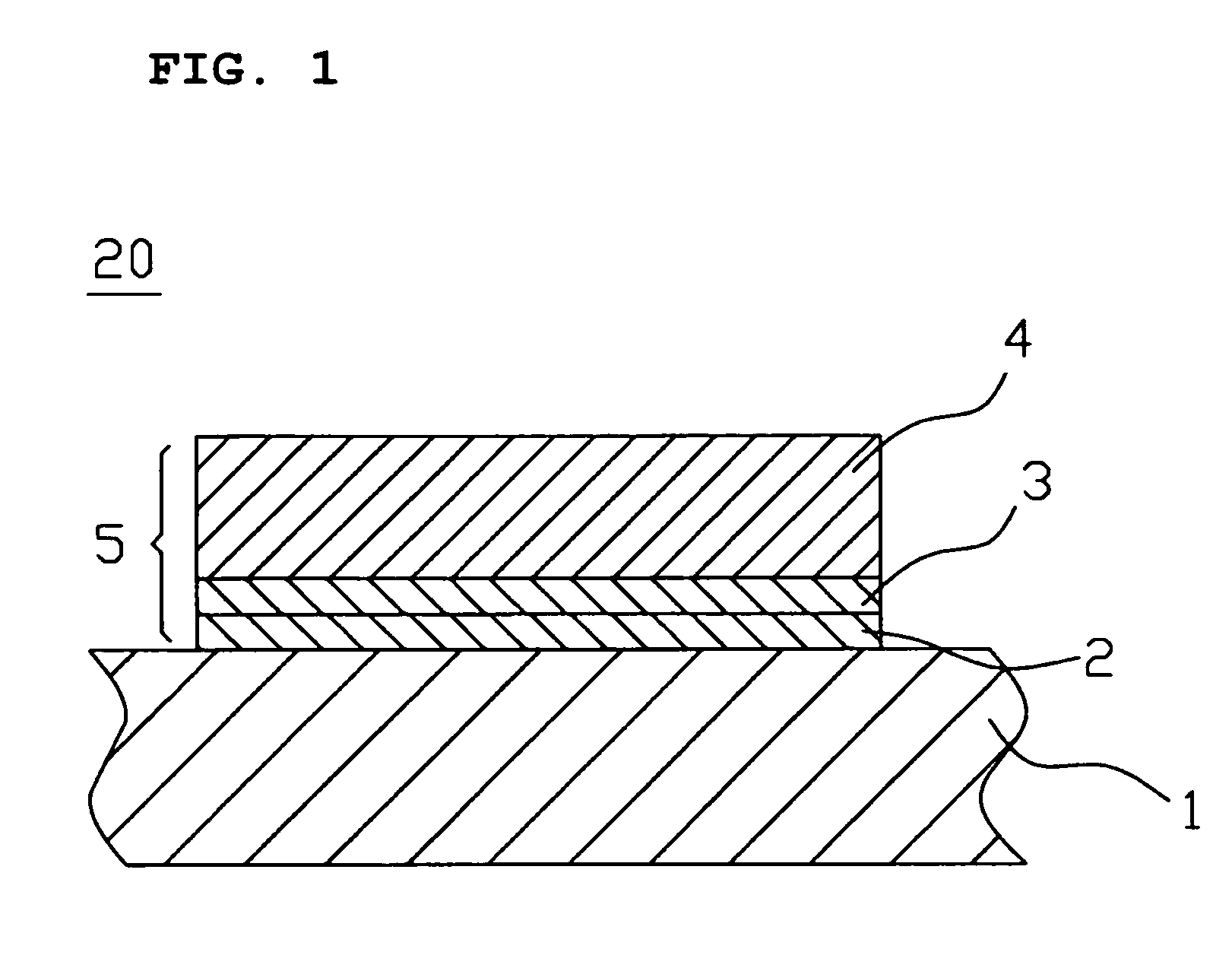
[0024]FIG. 1 illustrates a schematically sectional view of an example of the surface acoustic wave device manufactured by the manufacturing method of a preferred embodiment of the present invention.

[0025]A surface acoustic wave device 20 shown in FIG. 1 includes a piezoelectric substrate 1, a first electrode layer 2 on the piezoelectric substrate 1, a second electrode layer 3 on the first electrode layer 2, and a third electrode layer 4 on the second electrode layer 3.

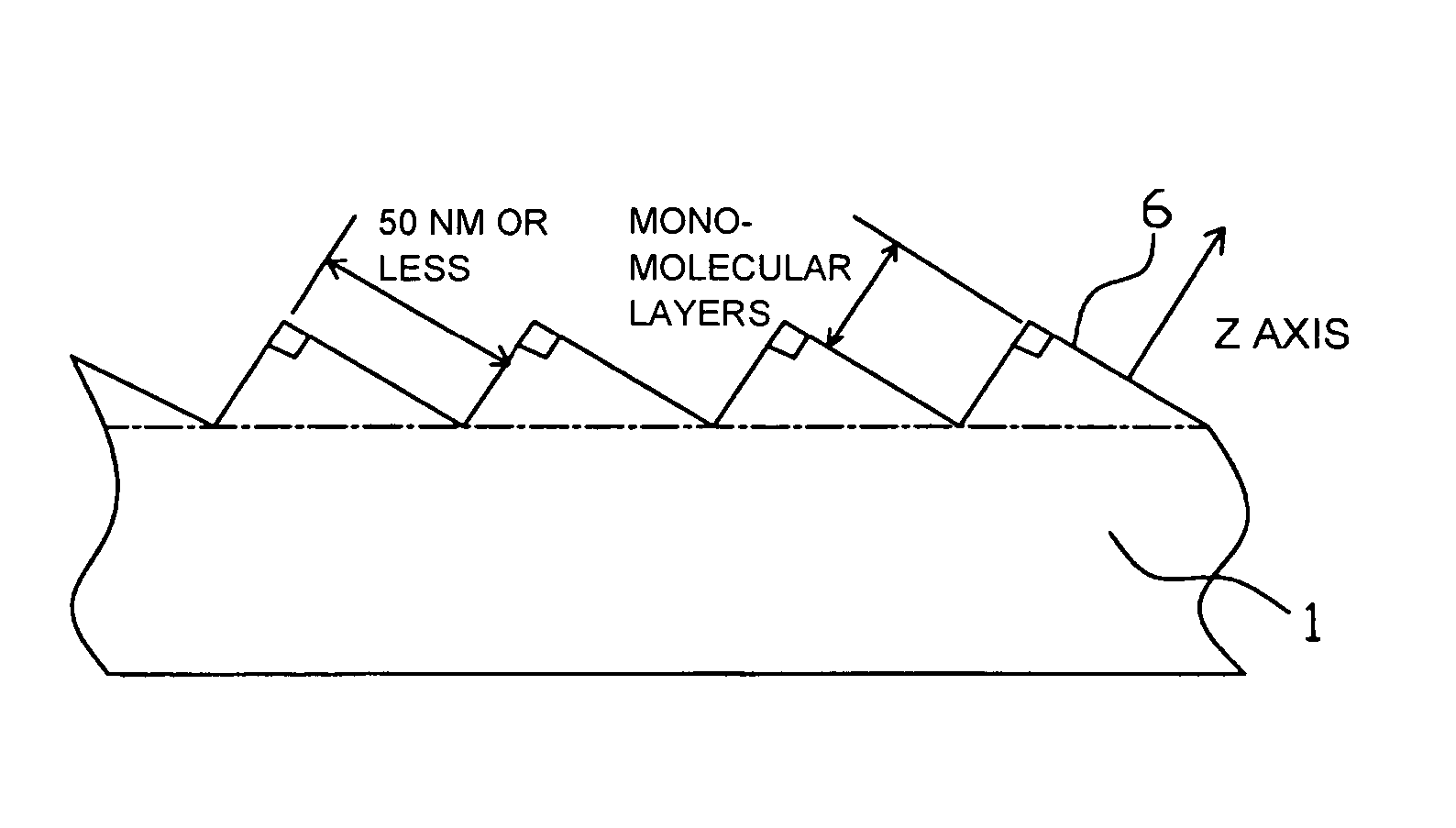
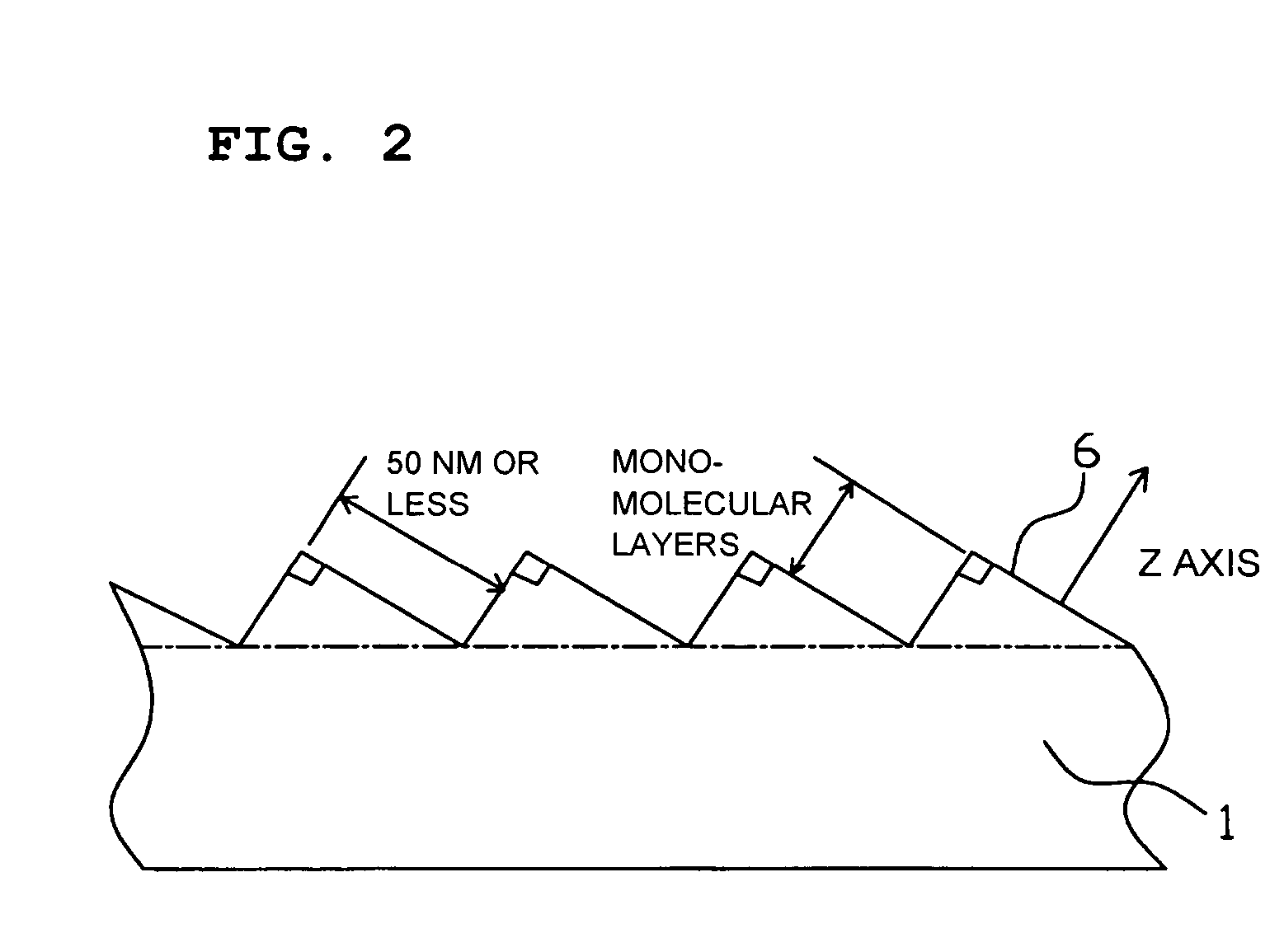
[0026]For the piezoelectric substrate 1, a θ°-rotated Y-cut X-propagation lithium niobate (LiNbO3) substrate or lithium tantalate (LiTaO3) substrate is preferably used. As shown in FIG. 2, the surface of the piezoelectric substrate 1 has a stepped structure including terraces having a width of about 50 nm or less, for example, and steps having a width of a mono-molecular layer.

[0027]A width of a mon...


PUM

PropertyMeasurementUnit
widthaaaaaaaaaa
surface temperatureaaaaaaaaaa

Abstract

A piezoelectric substrate is provided with interdigital transducer electrodes including a first electrode layer, a second electrode layer, and a third electrode layer that is principally made of aluminum. The piezoelectric substrate has a stepped structure on the surface of the piezoelectric substrate, the stepped structure including terraces each having a width of about 50 nm or less and steps each having a width of a mono-molecular layer (e.g., about 14 Å).

Description

BACKGROUND OF THE INVENTION[0001]1. Field of the Invention[0002]The present invention relates to a surface acoustic wave device such as a surface acoustic wave resonator and a surface acoustic wave filter, and a method for manufacturing the surface acoustic wave device, and more specifically, the present invention relates to a method for manufacturing a surface acoustic wave device provided with high-power durable electrodes for high-frequency operation and high-power operation.[0003]2. Description of the Related Art[0004]In recent years, surface acoustic wave devices including a desired electrode pattern disposed on a piezoelectric substrate have been widely used for surface acoustic wave filters and surface acoustic wave resonators with the development of mobile phones and mobile communication systems. The electrodes of the surface acoustic wave devices are made of aluminum from the outset of development due to a low specific gravity and a low electrical resistance of aluminum. On...

Claims


Application Information

Patent Timeline
Patent Type & Authority Patents(United States)
IPC IPC(8): H04R31/00H03H3/08H03H9/145
CPCH03H3/08Y10T29/42Y10T29/4908Y10T29/49002Y10T29/49005
Inventor NAKAGAWARA, OSAMUSHINODA, AKINORI
Owner MURATA MFG CO LTD
Why Eureka
Try Eureka