Switch circuit

Active Publication Date: 2013-07-04
MURATA MFG CO LTD
View PDF2 Cites 0 Cited by
  • Summary
  • Abstract
  • Description
  • Claims
  • Application Information

AI Technical Summary

Benefits of technology

[0010]The present invention makes it possible to improve the pow

Problems solved by technology

If the power durability of the switch SW is low, the following problem occurs.
However, there were p

Method used


Image

  • Switch circuit
  • Switch circuit
  • Switch circuit

Examples


first embodiment

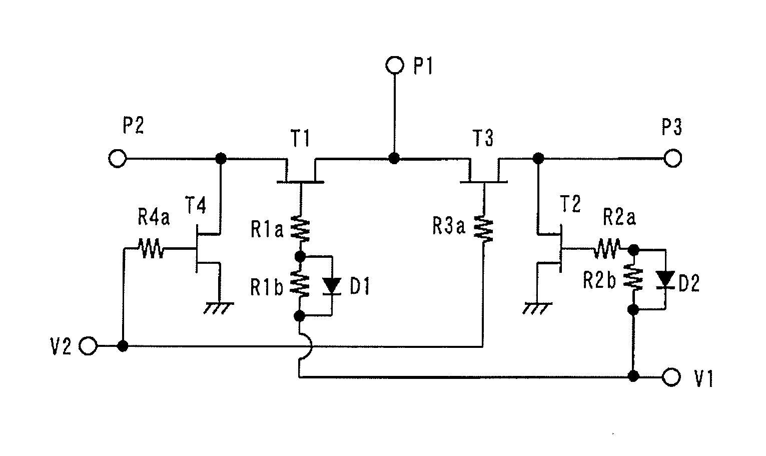
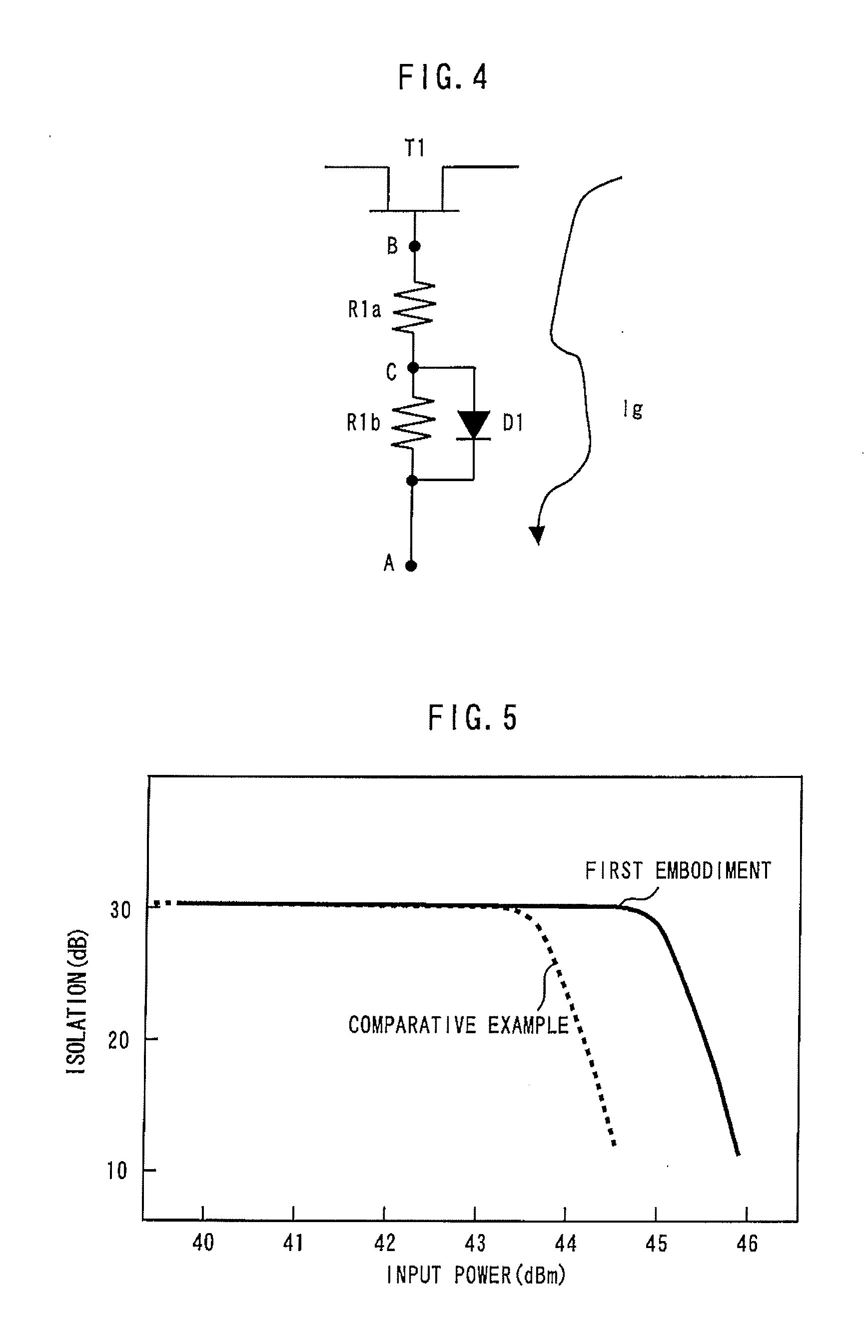
[0030]FIG. 1 is a circuit diagram showing a switch circuit according to the first embodiment of the present invention. Transistors T1 and T2, T3, and T4 are field-effect transistors used as switching elements. Control voltage applying terminals V1 and V2 are terminals for applying a control voltage for switching the switch. Resistors R1a, R1b, R2a, R2b, R3a, and R4a are isolation resistors having a resistance of several kΩ or more connected to the gates of respective transistors.

[0031]The transistor T1 is connected between an input-output terminal P1 and an input-output terminal P2. The transistor T2 is connected between an input-output terminal P3 and a grounding point. The transistor T3 is connected between an input-output terminal P1 and the input-output terminal P3. The transistor T4 is connected between the input-output terminal P2 and a grounding point. The control voltage applying terminal V1 is connected to the gates of transistors T1 and T2. The control voltage applying ter...

second embodiment

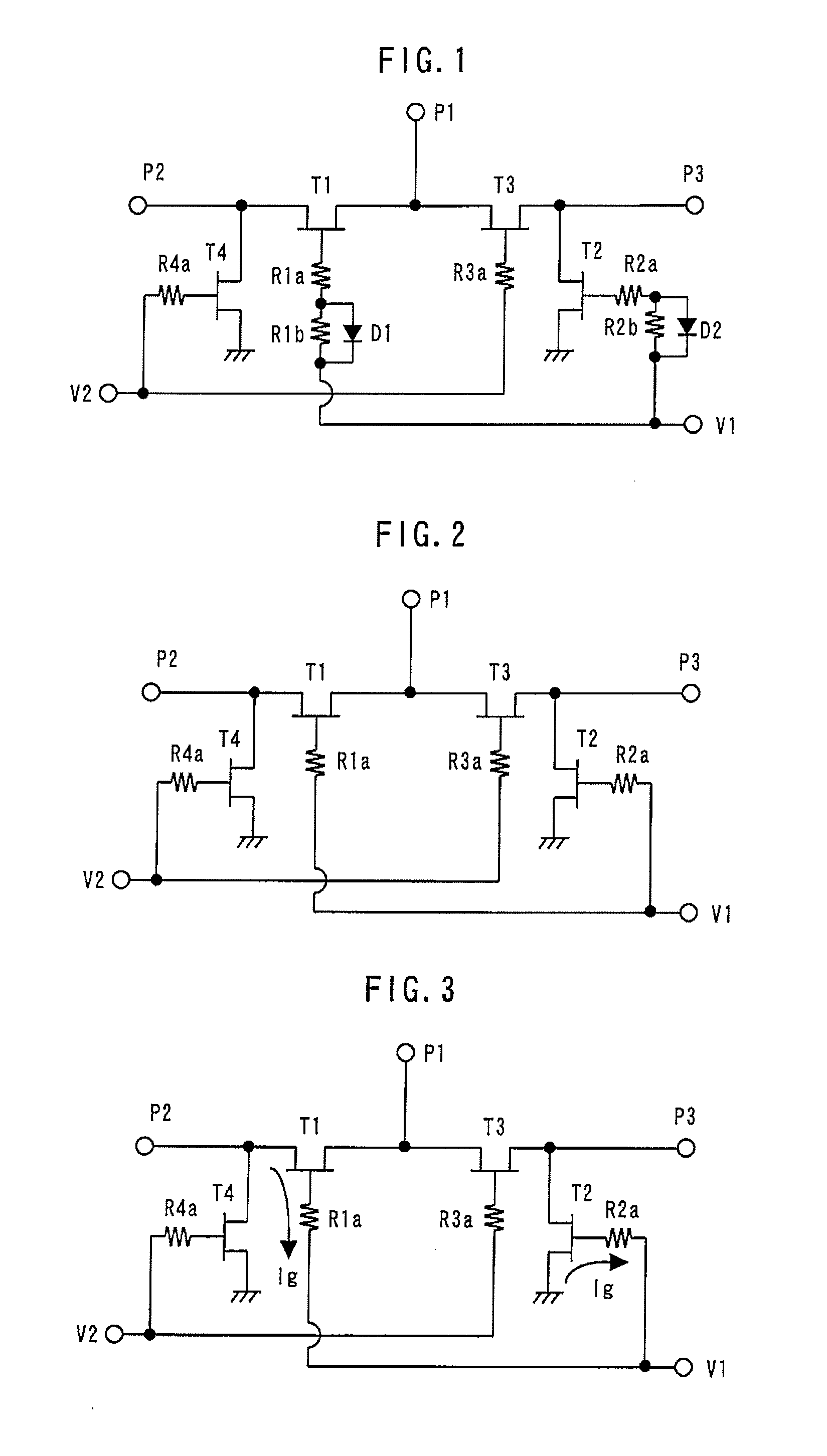
[0043]FIG. 7 is a circuit diagram showing a switch circuit according to the second embodiment of the present invention. In addition to the configuration in the first embodiment, resistors R3b and R4b are connected between the gate of the transistors T3 and T4, and the control voltage applying terminal V2, respectively. The diodes D3 and D4 are connected in parallel to the resistors R3b and R4b, respectively. The cathodes of the diodes D3 and D4 are connected to the control voltage applying terminal V2.

[0044]In the present embodiment, diodes are installed in parallel to a part of each gate resistor of the transistors in both paths of the switch. When these switch circuits are used in the system shown in FIG. 18, power durability to high power signals from the plural antennas in receiving are improved. As a result, the lowering of the signal switching accuracy of the switch circuits can be prevented.

[0045]FIG. 8 is a circuit diagram showing a modified example of the switch circuit acc...

third embodiment

[0046]FIG. 9 is a circuit diagram of a switch circuit according to the third embodiment of the present invention. In addition to the configuration of the first embodiment, the choke inductors L1 and L2 are connected to the resistors R1b and R2b in parallel, and connected to the diodes D1 and D2 in series, respectively. Here, since the gate current flows to the diodes D1 and D2, the resistors R1b and R2b connected in parallel are shorted. In order to prevent the lowering of impedance by choke inductors L1 and L2 at this time, the isolation function can be held.


PUM


Abstract

A switch circuit includes: first, second, and third input-output terminals; a first switching element connected between the first and second input-output terminals; a second switching element connected between the third input-output terminal and a grounding point; a third switching element connected between the first and third input-output terminals; a fourth switching element connected between the second input-output terminal and the grounding point; a first control voltage applying terminal connected to control terminals of the first and second switching elements; a second control voltage applying terminal connected to control terminals of the third and fourth switching elements; first and second resistors connected between the control terminals of the first and second switching elements and the first control voltage applying terminal, respectively; and first and second diodes connected in parallel with the first and second resistors, respectively, and having cathodes connected to the first control voltage applying terminal.

Description

BACKGROUND OF THE INVENTION[0001]1. Field of the Invention[0002]The present invention relates to a switch circuit mainly used in high-frequency band wireless communications equipment, high-frequency band radar equipment, and the like.[0003]2. Background Art[0004]A switch circuit is used in the system for transmitting signals in a high-frequency band, such as a micro-wave band or a millimeter band. FIGS. 17, 18, and 19 are diagrams of systems using switch circuits.[0005]In the system shown in FIG. 17, a switch SW is used for switching the transmitting and the receiving of signals. In the system shown in FIG. 18, a switch SW is used for switching signals from two antennas ANT. In the system shown in FIG. 19, a switch SW is used for preventing signals to be reflected from an antenna ANT and inputted into the receiver J1 when high-power signals are transmitted from the transmitter S1 in the system using a circulator CIR. Thereby, the receiver J1 containing a low noise amplifier can be p...

Claims


Application Information

Patent Timeline
IPC IPC(8): H03K17/56
CPCH03K17/693
Inventor TSUKAHARA, YOSHIHIRO
Owner MURATA MFG CO LTD
Why Eureka
Try Eureka