Photographic optical lens set, image capture device and electronic device
An optical lens and lens technology, which is applied in the field of miniaturized photographic optical lens sets and imaging devices, can solve the problems of large size, inability to meet the requirements of photographic systems, and concentrated light convergence ability.
- Summary
- Abstract
- Description
- Claims
- Application Information
AI Technical Summary
Problems solved by technology
Method used
Image

Examples
no. 1 example
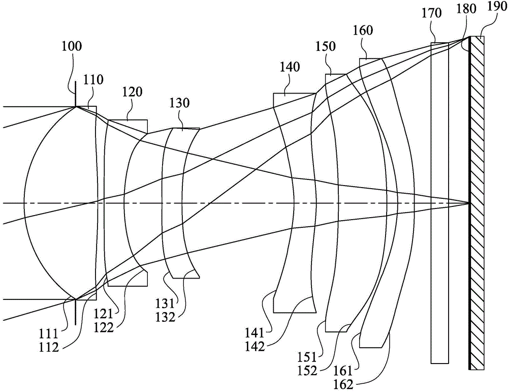
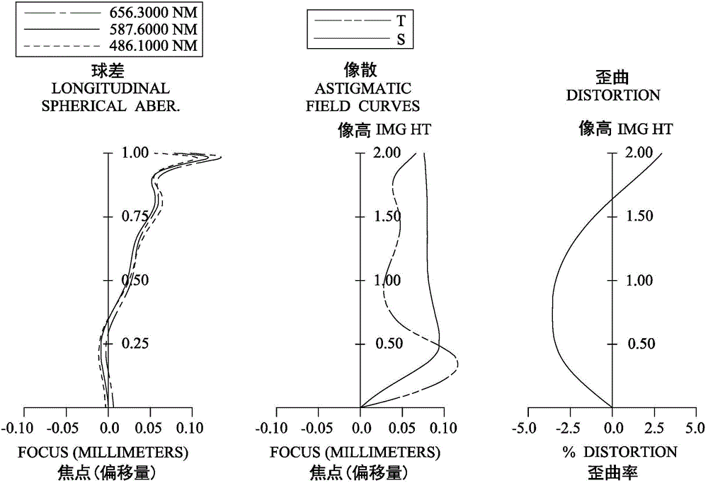
[0141] Please refer to figure 1 and figure 2 ,in figure 1 A schematic diagram showing an imaging device according to the first embodiment of the present invention, figure 2 From left to right are the spherical aberration, astigmatism and distortion curves of the first embodiment. Depend on figure 1 It can be seen that the image capturing device of the first embodiment includes an imaging optical lens set (not labeled separately) and an electronic photosensitive element 190 . The photographing optical lens group includes an aperture 100, a first lens 110, a second lens 120, a third lens 130, a fourth lens 140, a fifth lens 150, a sixth lens 160, an infrared filter The optical element 170 and the imaging surface 180, and the electronic photosensitive element 190 is arranged on the imaging surface 180 of the imaging optical lens group, wherein there are six lenses (110-160) with refractive power in the imaging optical lens group, and any two adjacent There is a distance be...
no. 2 example
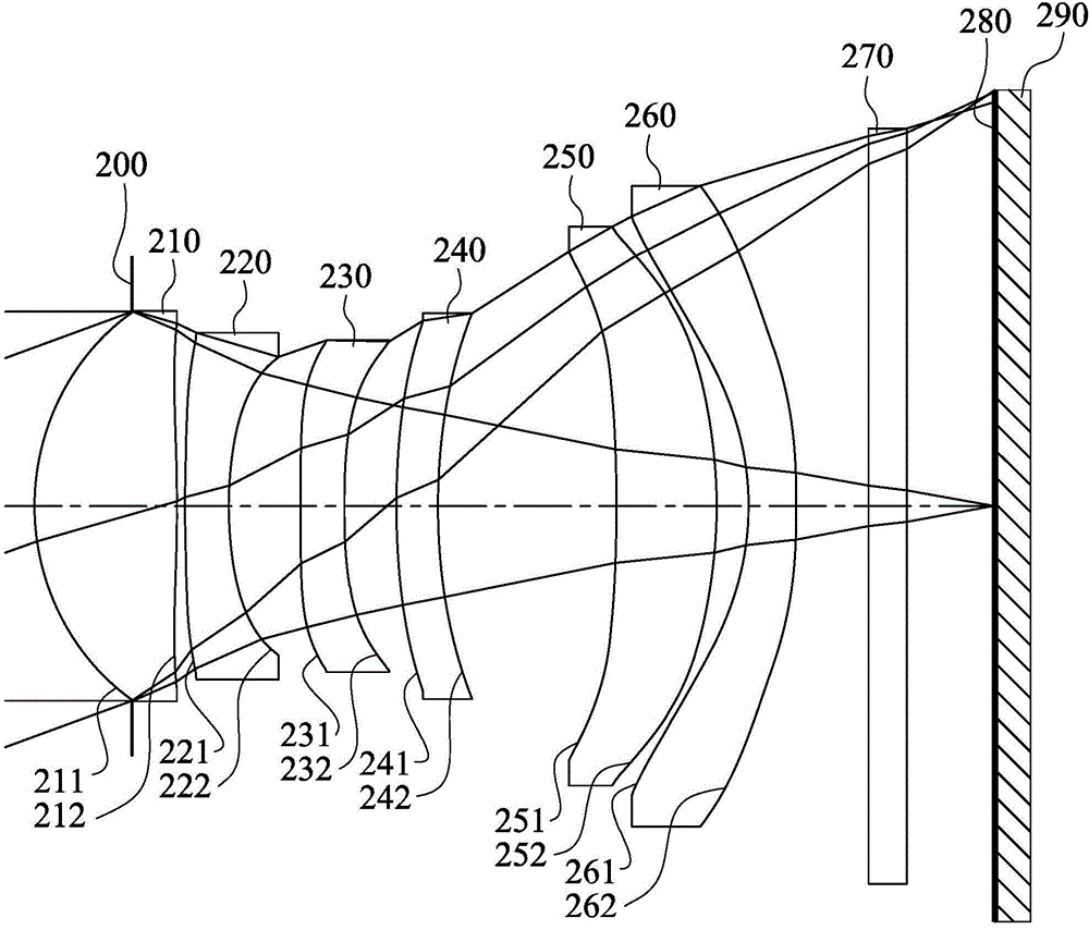
[0184] Please refer to image 3 and Figure 4 ,in image 3 A schematic diagram showing an imaging device according to a second embodiment of the present invention, Figure 4 From left to right are the spherical aberration, astigmatism and distortion curves of the second embodiment. Depend on image 3 It can be seen that the image capturing device of the second embodiment includes an imaging optical lens set (not labeled separately) and an electronic photosensitive element 290 . The photographing optical lens group includes aperture 200, first lens 210, second lens 220, third lens 230, fourth lens 240, fifth lens 250, sixth lens 260, infrared filter The optical element 270 and the imaging surface 280, and the electronic photosensitive element 290 is arranged on the imaging surface 280 of the imaging optical lens group, wherein there are six lenses (210-260) with refractive power in the imaging optical lens group, and any two adjacent There is a distance between the lenses ...
no. 3 example
[0201] Please refer to Figure 5 and Figure 6 ,in Figure 5 A schematic diagram showing an imaging device according to a third embodiment of the present invention, Figure 6 From left to right are the spherical aberration, astigmatism and distortion curves of the third embodiment. Depend on Figure 5 It can be seen that the image capturing device of the third embodiment includes an imaging optical lens set (not labeled separately) and an electronic photosensitive element 390 . The photographing optical lens group includes aperture 300, first lens 310, second lens 320, third lens 330, fourth lens 340, fifth lens 350, sixth lens 360, infrared filter The optical element 370 and the imaging surface 380, and the electronic photosensitive element 390 is arranged on the imaging surface 380 of the imaging optical lens group, wherein there are six lenses (310-360) with refractive power in the imaging optical lens group, and any two adjacent There is a distance between the lenses ...
PUM
 Abstract
Description
Claims
Application Information
 - R&D Engineer
- R&D Manager
- IP Professional
- Industry Leading Data Capabilities
- Powerful AI technology
- Patent DNA Extraction
Browse by: Latest US Patents, China's latest patents, Technical Efficacy Thesaurus, Application Domain, Technology Topic.
© 2024 PatSnap. All rights reserved.Legal|Privacy policy|Modern Slavery Act Transparency Statement|Sitemap