Supercharge Your Innovation With Domain-Expert AI Agents!

Optical Proximity Correction Method

A technology of optical proximity correction and target correction, which is applied in optics, original parts for photomechanical processing, instruments, etc., can solve the problems of long cycle time of optical proximity correction process, affecting production efficiency, and prone to deformation, etc., to achieve shortening Effects of computing time, improving productivity, and shortening cycle time

Active Publication Date: 2020-03-24
SEMICON MFG INT (SHANGHAI) CORP +1
View PDF4 Cites 0 Cited by
  • Summary
  • Abstract
  • Description
  • Claims
  • Application Information

AI Technical Summary

Problems solved by technology

[0004] At present, the normal condition model (normal condition model) is usually used for optical proximity correction, that is, to measure the edge position error (Edge Placement Error, referred to as EPE), while the process window (ProcessWindow, referred to as PW) model (PW condition model) is usually used for Post OPC verification after optical proximity correction. Some target points under the model under normal conditions become weak points under the model of process window conditions. Points are areas that are prone to deformation and distortion. These points need to adjust the correction target, then perform optical proximity correction again, and then perform optical proximity correction calibration again, and so on. Weaknesses are eliminated, and the process of removing these weaknesses will cause a longer cycle time in the optical proximity correction process, which will affect the efficiency of production, and the production cost will be higher

Method used


Image

  • Optical Proximity Correction Method
  • Optical Proximity Correction Method
  • Optical Proximity Correction Method

Examples


Embodiment Construction

[0031] The present invention will be further described below with reference to the drawings and specific embodiments, but it is not a limitation of the present invention.

[0032] figure 1 It is a schematic flow diagram of the optical proximity correction method of the present invention, such as figure 1 Shown:

[0033] This embodiment relates to an optical proximity correction method, which is applied to the process of the 45nm technology node in the semiconductor manufacturing process, for example, applied to the process of forming a metal layer (metal layer), including the following steps:

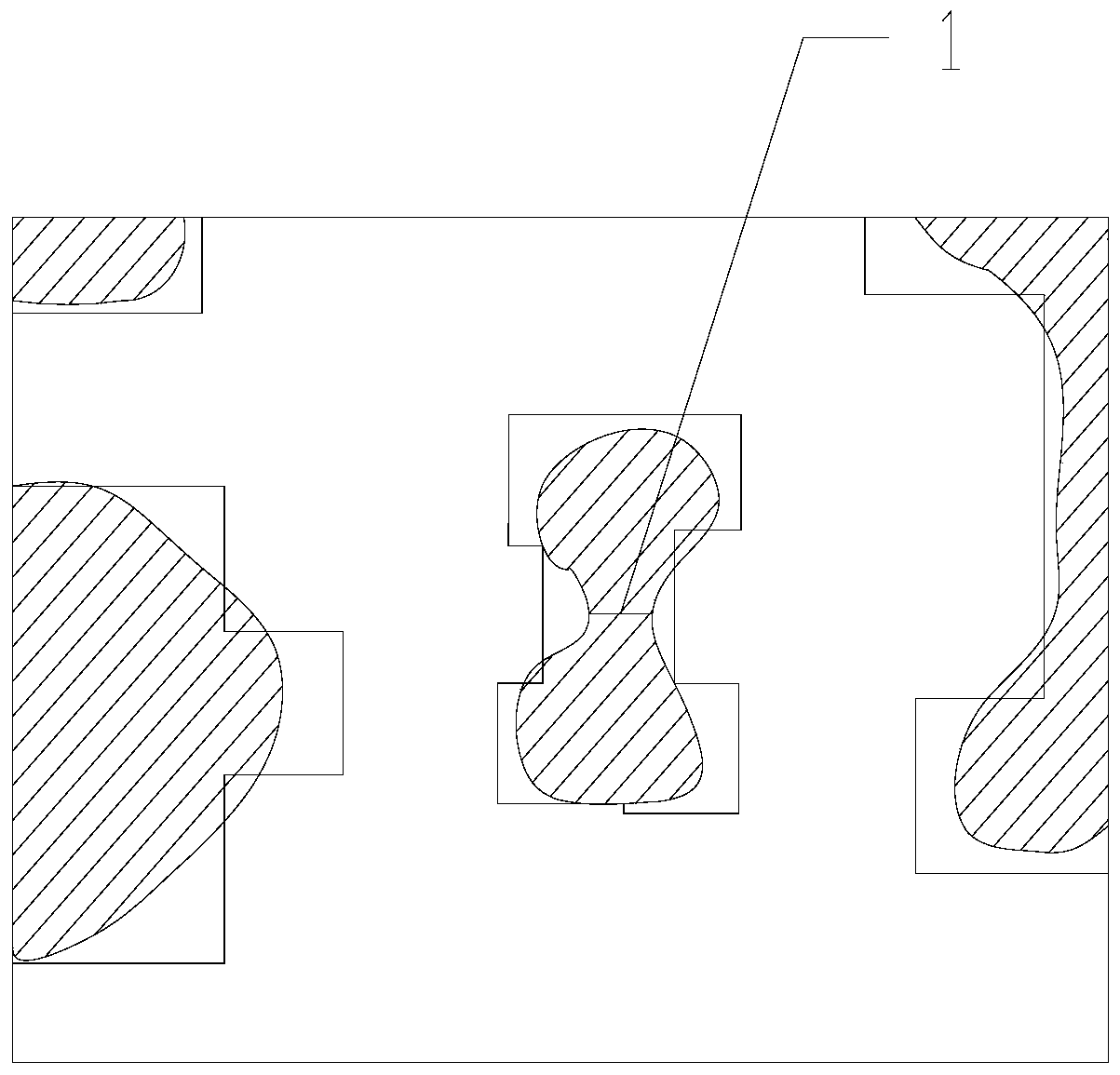
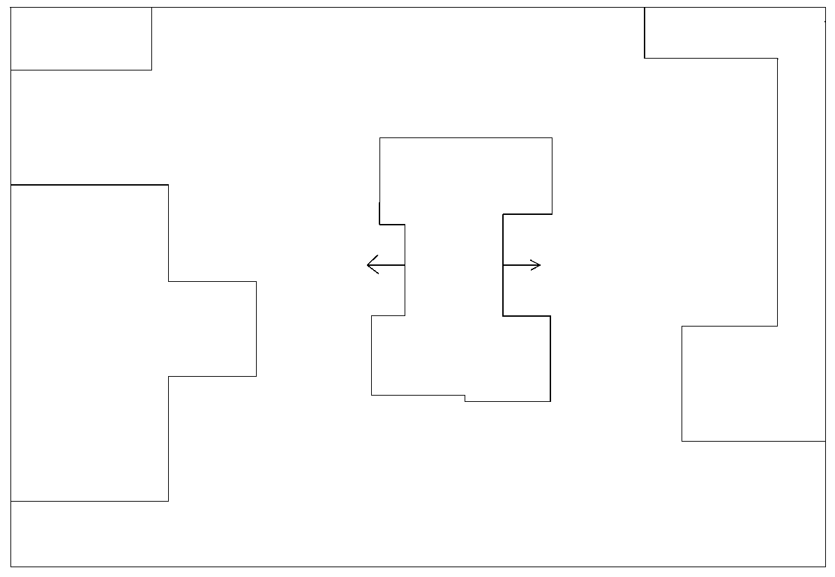
[0034] Step S1, input the designed mask data into a graphic data system (Input Graphic Data System, Input GDS) to generate a target graphic for optical proximity correction, that is, a graphic to be corrected.

[0035] Step S2: Use a normal condition model to perform first optical proximity correction on the pattern to be corrected to obtain a first correction pattern, that is, an initial correc...


PUM


Abstract

The invention discloses an optical proximity correction method. The method is characterized in that first optical proximity correction is executed on a graph to be corrected to obtain a first correction graph, the first correction graph is verification by employing a model having a largest space value and a model having a smallest linewidth value selected in a process window model corresponding to the processes, a point with easy deviation is determined, the point is performed with target correction, second optical proximity correction is executed to obtain a second correction graph, the process window model is used for examining the second correction graph, performing modification on the first correction graph during optical proximity correction, thereby the point with easy deviation is timely discovered and corrected, redundant operation data volume for the subsequent optical proximity correction is reduced, data operation time of a mask layer is shortened, the cycling correction for redetermining the optical proximity corrective target graph is not required, a period for the optical proximity correction is shortened, and production efficiency is increased.

Description

Technical field [0001] The invention relates to the technical field of semiconductor manufacturing, and in particular to an optical proximity correction method. Background technique [0002] A mask is a necessary device in the photolithography process of integrated circuit manufacturing. The mask mainly includes a transparent glass substrate and a pattern to be exposed composed of a non-transparent material (generally chromium) covering the glass substrate. During photolithography, the mask is placed between the radiation source and the focusing lens. The light emitted by the radiation source passes through the mask, passes through the lens, and irradiates the surface of the wafer with photoresist spin-coated on the surface of the wafer. The photoresist is selectively exposed, so that the pattern on the mask is mapped to the photoresist layer. [0003] When the light emitted by the radiation source passes through the mask, it is affected by the edge of the pattern to be exposed (...

Claims


Application Information

Patent Timeline
Patent Type & Authority Patents(China)
IPC IPC(8): G03F1/36
Inventor 王兴荣张迎春
Owner SEMICON MFG INT (SHANGHAI) CORP
Features
  • R&D
  • Intellectual Property
  • Life Sciences
  • Materials
  • Tech Scout
  • Unparalleled Data Quality
  • Higher Quality Content
  • 60% Fewer Hallucinations
Learn More