Chip on film and display device

A chip-on-film and display device technology, which is applied to electrical components, electrical solid-state devices, circuits, etc., can solve the problems of being easily squeezed, the component 41 is crushed, and the width of the display device frame is increased, so as to reduce crushing, thickness, etc. Thin, yield-enhancing effect

Inactive Publication Date: 2016-08-03
BOE TECH GRP CO LTD
View PDF3 Cites 35 Cited by
  • Summary
  • Abstract
  • Description
  • Claims
  • Application Information

AI Technical Summary

Problems solved by technology

figure 1 It is a structural diagram of a chip-on-chip film in the prior art. The flexible circuit board 20 includes a base 21, a metal layer 22 and a paint film 23. The paint film 23 exposes both ends of the metal layer 22, and the exposed two parts are connected to the display substrate 30 and the display substrate 30 respectively. printed circuit board 40 binding, such as figure 2 As shown; for a bottom-emission organic light-emitting display device, after the flexible circuit board 20 is bound to the display substrate 30 and the printed circuit board 40 respectively, the flexible circuit board 20 is bent toward the side of the display substrate 30 away from the light-emitting direction After, such as image 3 As shown, it is easy to cause the following problems: the driver chip 10 on the flexible circuit board 20 is exposed outside, which is easy to be squeezed, and causes the frame width of the display device to increase; the components 41 on the printed circuit board 40 and the printed circuit board 40 The binding areas are located on different sides, and when the printed circuit board 40 is bound to the flexible circuit board 20, it is easy to cause crush damage to the component 41; in addition, after the flexible circuit board 20 is bent, the printed circuit board 40 is located above the flexible circuit board 20, Therefore, when the bending degree of the flexible circuit board 20 is constant, the overall thickness of the display device is relatively large.

Method used


Image

  • Chip on film and display device
  • Chip on film and display device
  • Chip on film and display device

Examples


Embodiment Construction

[0024] Specific embodiments of the present invention will be described in detail below in conjunction with the accompanying drawings. It should be understood that the specific embodiments described here are only used to illustrate and explain the present invention, and are not intended to limit the present invention.

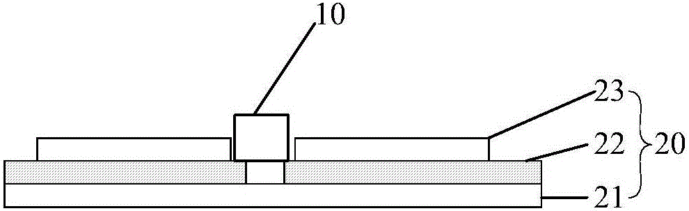
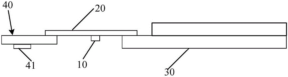
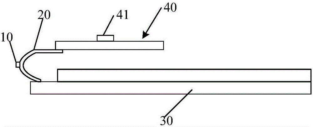
[0025] As an aspect of the present invention, a chip-on-chip film is provided, such as Figure 4 with Figure 5 As shown, the chip-on-film includes a flexible circuit board 60, and the flexible circuit board 60 includes a conductive layer 62, and the conductive layer 62 includes a first binding region 621 located at the first end of the conductive layer 62 and a first bonding area 621 located at the second end of the conductive layer. 62 of the second binding area 622, the first binding area 621 is used for binding (bonding) display substrate 30, the second binding area 622 is used for binding printed circuit board 40, the first binding area 621 and the second ...


PUM


Abstract

The present invention provides a chip on film. The chip on film comprises a flexible circuit board, and the flexible circuit board includes a conductive layer consisting of a first binding zone located at the first end of the conductive layer and a second binding zone located at the second end of the conductive layer; the first binding zone is configured to bind a display substrate, and the second binding zone is configured to bind a printing circuit board, wherein the first binding zone and the second binding zone are respectively located at two opposite surfaces of the conductive layer. Correspondingly, the present invention further provides a display device. The chip on film and the display device are able to reduce the whole thickness of the display device and prevent the chip on the chip on film from being extruded.

Description

technical field [0001] The invention relates to the field of display technology, in particular to a chip-on-chip film and a display device. Background technique [0002] The chip-on-chip technology (ChipOnFlex, or, ChipOnFilm, COF) is a technology of bonding the pads on the driver chip and the pins on the flexible circuit board by thermal compression. figure 1 It is a structural diagram of a chip-on-chip film in the prior art. The flexible circuit board 20 includes a base 21, a metal layer 22 and a paint film 23. The paint film 23 exposes both ends of the metal layer 22, and the exposed two parts are connected to the display substrate 30 and the display substrate 30 respectively. printed circuit board 40 binding, such as figure 2 As shown; for a bottom-emission organic light-emitting display device, after the flexible circuit board 20 is bound to the display substrate 30 and the printed circuit board 40 respectively, the flexible circuit board 20 is bent toward the side of...

Claims


Application Information

Patent Timeline
Patent Type & Authority Applications(China)
IPC IPC(8): H01L27/32
CPCH10K59/12
Inventor 解红军
Owner BOE TECH GRP CO LTD
Why Eureka
Try Eureka