Display apparatus and manufacturing method therefor

A production method and technology of a display device, which are applied to casings with display/control units, instruments, static electricity, etc., can solve the problems of inability to meet the minimum certification standards of mobile terminals, performance degradation, etc., and achieve easy surface attachment conditions and products. Yield and performance improvements, easy-to-check effects

Active Publication Date: 2016-08-10
BOE TECH GRP CO LTD +1
View PDF7 Cites 4 Cited by
  • Summary
  • Abstract
  • Description
  • Claims
  • Application Information

AI Technical Summary

Problems solved by technology

For example, the anti-ESD specification of driver chips currently on the market is about 2kV, but due to the constraints of existing technologies, it cannot meet the minimum certification standards for mobile terminals (generally 6-8kV), which leads to the overall performance of this type of display products decline

Method used


Image

  • Display apparatus and manufacturing method therefor
  • Display apparatus and manufacturing method therefor
  • Display apparatus and manufacturing method therefor

Examples


Embodiment Construction

[0030] In order to make the purpose, technical solutions and advantages of the embodiments of the present invention clearer, the technical solutions in the embodiments of the present invention will be clearly and completely described below in conjunction with the drawings in the embodiments of the present invention. Obviously, the described embodiments It is a part of embodiments of the present invention, but not all embodiments. Based on the embodiments of the present invention, all other embodiments obtained by persons of ordinary skill in the art without creative efforts fall within the protection scope of the present invention.

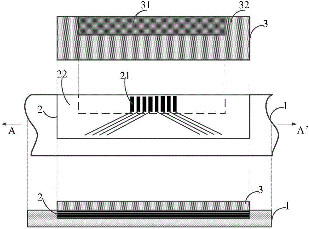
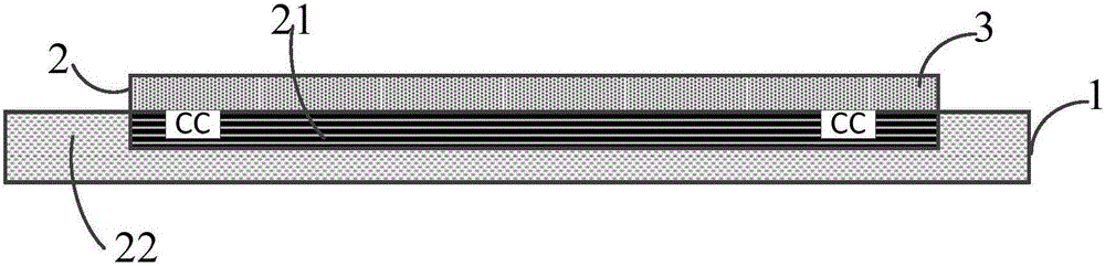
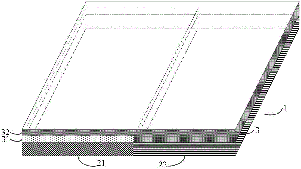
[0031] An embodiment of the present invention provides a manufacturing method of a display device, the manufacturing method comprising: attaching an electrostatic shielding layer 3 on the edge area 2 of the display panel 1 where the connection line pattern is exposed. Such as figure 1 As shown, wherein the insulating material region 31 on the sur...


PUM


Abstract

Embodiments of the invention provide a display apparatus and a manufacturing method therefor. The manufacturing method comprises the steps of attaching a static shielding layer to an edge region of a connecting line pattern, wherein the connecting line pattern is exposed on a display panel; the static shielding layer is provided with an insulating material region; the insulating material region is in contact with the region where the connecting line pattern is located; and the other region, except the region where the connecting line pattern is located, in the edge region is in contact with a conductive material region on the surface of the static shielding layer. The display apparatus provided by the embodiments of the invention is prepared by the manufacturing method; the anti-ESD (electrostatic discharge) capability of the chip connecting line position on the edge can be improved without increasing technological processes; in addition, the formed material, including the metal static shielding layer, is non-transparent; compared with a photo-sensitive resist, the surface attaching condition of the static shielding layer is easier to detect, and surface flatness defects cannot be formed easily; and the yield and improvement of the performance of the product can be facilitated.

Description

technical field [0001] The invention relates to the field of display technology, in particular to a display device and a manufacturing method thereof. Background technique [0002] For FIC (Film Integrated Circuit, film integrated circuit) products, electrostatic discharge (Electro-Static discharge, ESD) is likely to cause damage and damage to the products. For a display device, a driver IC is an important circuit component. In practical applications, due to the requirements of the manufacturing process, a layer of photosensitive glue (photosensitive glue) will be coated on the metal terminal area of ​​the driver chip. Photosensitive adhesive can prevent metal terminals from short-circuiting in contact with conductors, but photosensitive adhesive is transparent, it is not easy to check its surface smoothness and has little effect on anti-ESD. [0003] However, at present, the anti-ESD capability of the driver chip has become one of the important reference factors for the a...

Claims


Application Information

Patent Timeline
Patent Type & Authority Applications(China)
IPC IPC(8): H05F1/02
CPCH05F1/02G02F1/13452G02F1/136204H05F3/04H05K5/0017H05K9/0067
Inventor 徐敬义李鑫张琨鹏樊祎任艳伟赵艳艳刘宇
Owner BOE TECH GRP CO LTD
Why Eureka
Try Eureka