Liquid crystal display panel

A liquid crystal display panel and display area technology, applied in nonlinear optics, instruments, optics, etc., can solve problems such as poor display, entry into the liquid crystal layer, mutual dissolution and puncture of frame glue, etc.

Inactive Publication Date: 2016-08-24
XIAMEN TIANMA MICRO ELECTRONICS +1
View PDF6 Cites 18 Cited by
  • Summary
  • Abstract
  • Description
  • Claims
  • Application Information

AI Technical Summary

Problems solved by technology

At this time, the liquid crystal molecules and the uncured frame glue are prone to mutual dissolution and puncture.
That is to say, the uncured sealant may spread to the display area and enter the liquid crystal layer under the action of extrusion, resulting in poor display

Method used


Image

  • Liquid crystal display panel
  • Liquid crystal display panel
  • Liquid crystal display panel

Examples


Embodiment Construction

[0021] The application will be further described in detail below in conjunction with the accompanying drawings and embodiments. It should be understood that the specific embodiments described here are only used to explain related inventions, rather than to limit the invention. It should also be noted that, for ease of description, only parts related to the invention are shown in the drawings.

[0022] It should be noted that, in the case of no conflict, the embodiments in the present application and the features in the embodiments can be combined with each other. The present application will be described in detail below with reference to the accompanying drawings and embodiments.

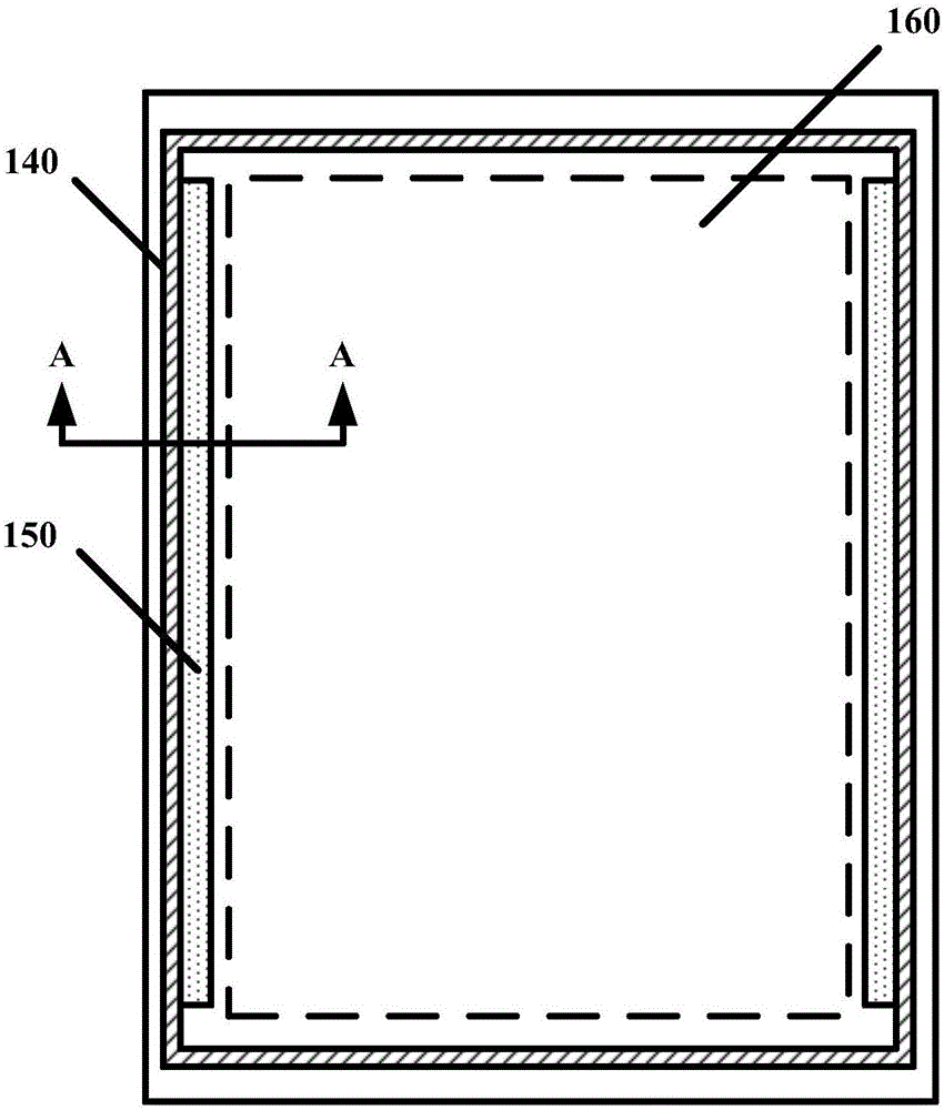
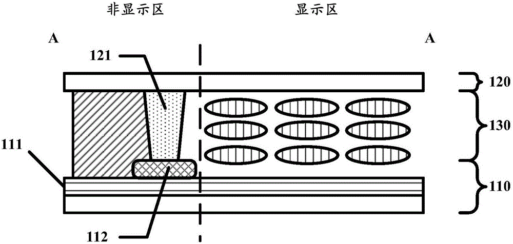
[0023] see figure 1 Shown is a schematic structural diagram of an embodiment of the liquid crystal display panel of the present application, figure 2 for along figure 1 Sectional view of A-A in Fig.

[0024] Below, combine figure 1 and figure 2 Now, the liquid crystal display panel of this ...


PUM


Abstract

The application discloses a liquid crystal display panel, comprising an array substrate, a color film substrate opposite to the array substrate, a liquid crystal layer formed between the array substrate and the color film substrate, and frame plastic for fixing the array substrate and the color film substrate; the array substrate includes a thin-film transistor device layer and a first film layer formed on the same; the liquid crystal display panel also comprises a support structure formed between the array substrate and the color film substrate, wherein the support structure comprises support posts formed on the color film substrate and a pad formed on the first film layer; the liquid crystal display panel includes a display area and a non-display area surrounding the display area; the support posts and the pad are positioned in the non-display area of the liquid crystal display panel and contact each other. According to the scheme of the embodiments of the application, it is possible to avoid mutual fusion and piercing of the frame plastic and liquid crystal, preventing poor displaying caused thereby.

Description

technical field [0001] The present disclosure generally relates to the field of display technology, and in particular, relates to a liquid crystal display panel. Background technique [0002] In the existing methods for manufacturing liquid crystal display panels, usually a plurality of array substrates are fabricated on a glass substrate, and a plurality of color filter substrates are fabricated on another glass substrate. [0003] Next, liquid crystal is dripped into the display area of ​​the array substrate, and a sealant is coated on the non-display area of ​​the color filter substrate. The sealant is in a closed shape surrounding the display area. Next, the array substrate is aligned with the color filter substrate, so that the sealant and the planarization layer of the array substrate are pressed to form a display panel. In the display panel, a closed liquid crystal cell is formed between the array substrate and the color filter substrate, and the liquid crystal cell ...

Claims


Application Information

Patent Timeline
Patent Type & Authority Applications(China)
IPC IPC(8): G02F1/1339
CPCG02F1/13394G02F1/133388G02F2201/501G02F1/133351G02F1/1339G02F1/13415G02F1/136295G02F1/133345G02F1/133514G02F1/136286G02F1/1368G02F2202/28
Inventor 颜佳友周秀峰李俊谊刘冰萍郑丽华文亮陈国照沈柏平
Owner XIAMEN TIANMA MICRO ELECTRONICS
Why Eureka
Try Eureka