Electronic device manufacturing method, display device manufacturing method, photomask manufacturing method and photomask

A manufacturing method and technology for electronic devices, which are applied in the fields of semiconductor/solid-state device manufacturing, electrical components, and photoengraving processes of patterned surfaces, etc., can solve problems such as device malfunction, and achieve the effect of improving coincidence accuracy.

Active Publication Date: 2016-08-24
HOYA CORP
View PDF7 Cites 0 Cited by
  • Summary
  • Abstract
  • Description
  • Claims
  • Application Information

AI Technical Summary

Problems solved by technology

However, when there are misalignment error components in different directions, the amount of misalignment that may cause device malfunction may be generated due to their accumulation.

Method used


Image

  • Electronic device manufacturing method, display device manufacturing method, photomask manufacturing method and photomask
  • Electronic device manufacturing method, display device manufacturing method, photomask manufacturing method and photomask
  • Electronic device manufacturing method, display device manufacturing method, photomask manufacturing method and photomask

Examples


Embodiment 1

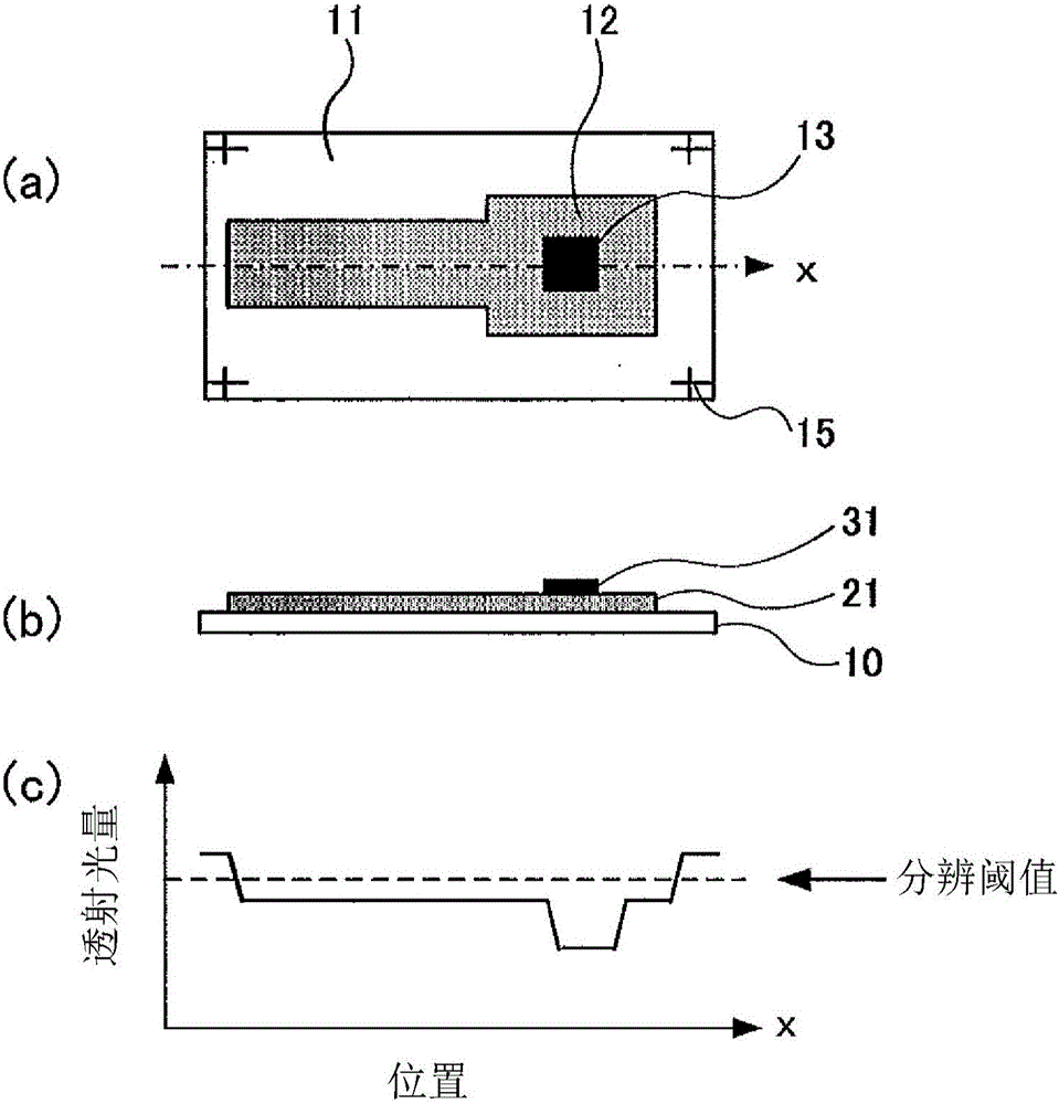
[0151] figure 1 One mode of a photomask that can be used in the method of manufacturing an electronic device according to Example 1 of the present invention is shown. figure 1 (a) shows the first transfer pattern including the light-transmitting portion 11, the semi-transmitting portion 12, and the light-shielding portion 13 which the photomask has in plan view, figure 1 (b) shows the cross section of the dotted line part in (a).

[0152] Prepare a photomask blank obtained by sequentially forming a light semitransmissive film 20 and a light shielding film 30 on a transparent substrate 10, and pattern the light semitransmissive film 20 and light shielding film 30 through a photolithography process to form figure 1 Photomask shown. Therefore, the transparent substrate 10 is exposed at the light-transmitting part 11, the semi-transparent part 12 is formed by forming the semi-transparent film pattern 21 on the transparent substrate 10, and the light-shielding part 13 is formed b...

Embodiment 2

[0170] In Example 2, similarly to Example 1, the same photomask was used to pattern the first thin film 60 and the second thin film 70, thereby forming the same electronic device as in Example 1. However, the shape of the first transfer pattern that the photomask has, and the photosensitivity of the first resist and the second thin film 70 formed on the transfer target are different from those in Example 1.

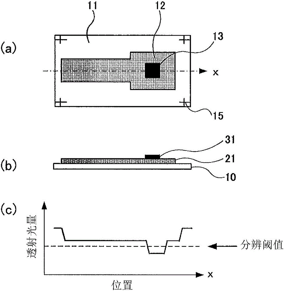
[0171] As the first transfer pattern of the photomask used here, use Figure 5 The pattern for the first transfer shown (it is different from that described later Figure 7 The photomask for is the same photomask). Figure 5 (a) is a top view, Figure 5 (b) is a cross-sectional view, Figure 5 (c) shows the transmitted light amount distribution of exposure light.

[0172] Similar to the photomask of Example 1, a photomask blank obtained by sequentially forming the light semitransmissive film 20 and the light shielding film 30 on the transparent substrate 10 was prepar...

Embodiment 3

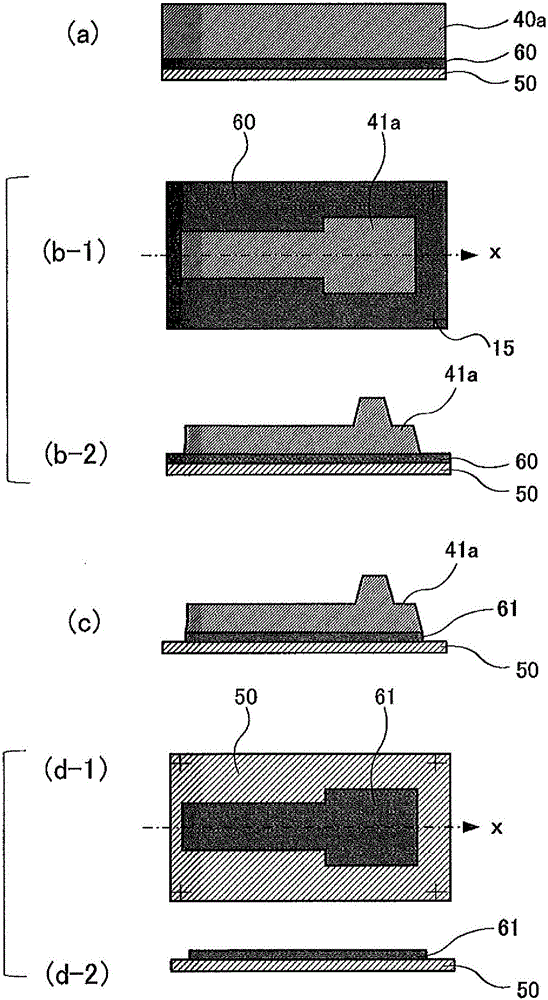
[0231] Figure 9 An example of a photomask used in the process of manufacturing an electronic device in Example 3 according to another aspect of the present invention is shown.

[0232] This photomask has a pattern for first transfer, and the pattern for first transfer is obtained by preparing a photomask obtained by forming a semitransmissive film 20 on a transparent substrate 10 and further forming a light shielding film 30 . The pattern for the first transfer is obtained by patterning the light-shielding film 30 on the mold body. The membrane material is the same as in Example 1.

[0233] The first transfer pattern is used to form the first thin film pattern 61 to form the connection portion in the source / drain layer. On the other hand, after the first thin film pattern 61 is formed, it can be used for additional processing The second transfer pattern used to form the second thin film pattern 71 .

[0234] The pattern for 1st transfer has the light shielding part 13 and ...


PUM

PropertyMeasurementUnit
widthaaaaaaaaaa
diameteraaaaaaaaaa

Abstract

The present invention provides an electronic device manufacturing method, a display device manufacturing method, a photomask manufacturing method and a photomask, which can reduce the alignment errors among layers. The electronic device manufacturing method is characterized by comprising the following steps of forming a first film pattern, and implementing a first photoetching process using a first photomask on a substrate; forming a second film pattern and implementing a second photoetching process using a second photomask, wherein the first and second photomasks comprise a first transfer pattern containing a light transmitting part, a shading part and a semi-light transmitting part, and are the same photomask, or the second photomask is the photomask of the second transfer pattern formed by processing the first transfer pattern possessed by the first photomask.

Description

[0001] The patent application of the present invention is a divisional case of the invention patent application with the title of "Manufacturing method of electronic device and display device, photomask and its manufacturing method", the application date is October 12, 2013, and the application number is "201310475805.7" Apply. technical field [0002] The present invention relates to a method of manufacturing an electronic device using photolithography, and more particularly to a method of manufacturing a display device. It also relates to a photomask used in the above-mentioned manufacturing method and its manufacturing method. Background technique [0003] Patent Document 1 describes a method for forming a pattern with good alignment accuracy in a manufacturing process of an electro-optical device or a semiconductor device. Patent Document 1 describes a method of measuring the amount of deviation between the center of the alignment mark on the upper layer and the center ...

Claims


Application Information

Patent Timeline
Patent Type & Authority Applications(China)
IPC IPC(8): G03F1/80H01L21/027
CPCG03F1/80H01L21/027H01L21/0274G03F1/20
Inventor 山口昇
Owner HOYA CORP
Why Eureka
Try Eureka