

Deposition apparatus, deposition method, and organic electroluminescent element manufacturing method
A technology of evaporation and evaporation source, which is applied in the manufacture of electroluminescent light sources, electrical components, semiconductor/solid-state devices, etc. It can solve the problems of low water resistance and unsuitability for wet treatment, and achieve the effect of excellent control accuracy
- Summary
- Abstract
- Description
- Claims
- Application Information
AI Technical Summary
Problems solved by technology
Method used
Image

Examples
Embodiment approach 1
[0072] In this embodiment mode, a method of manufacturing a bottom-emission organic EL element that takes out light from the TFT substrate side and performs RGB full-color display and an organic EL display having an organic EL element manufactured by this manufacturing method will be mainly described. The method is also applicable to the manufacturing methods of other types of organic EL elements.
[0073] First, the overall structure of the organic EL display of this embodiment will be described.
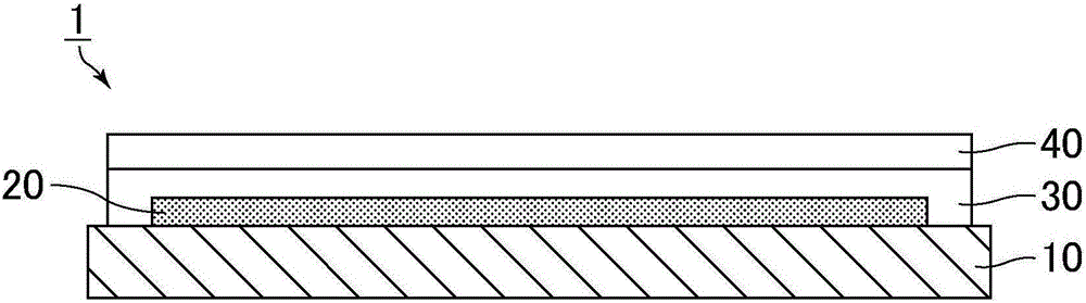
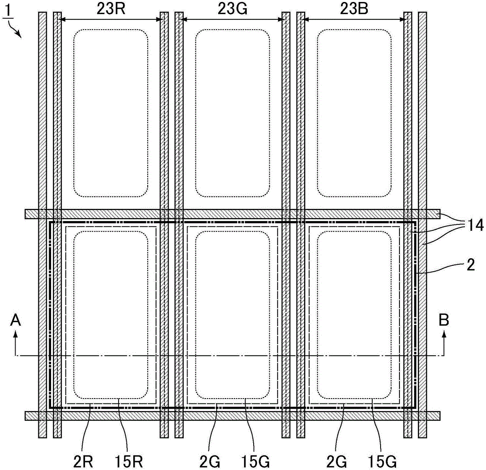
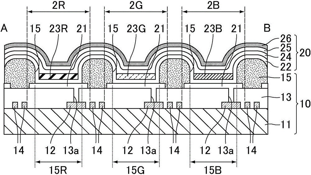
[0074] figure 1 It is a schematic cross-sectional view of an organic EL display having an organic EL element produced by the method for producing an organic EL element according to Embodiment 1. figure 2 yes means figure 1 A schematic plan view of the structure within the display region of the organic EL display shown. image 3 yes means figure 1 A schematic cross-sectional view of the structure of the TFT substrate of the organic EL display shown, equivalent to figure 2 ...
Embodiment approach 2
[0203] This embodiment is substantially the same as Embodiment 1 except that the feedback control by the first control system is omitted. Therefore, in this embodiment, the features unique to this embodiment will be mainly described, and the description of content overlapping with that of Embodiment 1 will be omitted. In addition, in this embodiment and Embodiment 1, the same code|symbol is attached|subjected to the component which is the same or has the same function.
[0204] In this embodiment, the feedback control by the 1st control system is abbreviated and the output of the heating apparatus 120 is fixed to a predetermined value from a viewpoint of cost reduction significantly. In this case, as in Embodiment 1, the vapor deposition rate on the substrate 130 can be controlled with high precision in the entire vapor deposition region by the second control system. However, if only correction of the second vapor deposition rate is performed by the second control system in a...
Embodiment approach 3
[0206] This embodiment is substantially the same as Embodiment 1 except that one of the film thickness monitoring units 101 and 102 is omitted. Therefore, in this embodiment, the features unique to this embodiment will be mainly described, and the description of the contents overlapping with Embodiment 1 will be omitted. In addition, in this embodiment and Embodiment 1, the same code|symbol is attached|subjected to the component which is the same or has the same function.
[0207] In the present embodiment, the control accuracy is lowered, but from the viewpoint of cost reduction, the deposition is performed while controlling the distance Ts between the substrate deposition sources and the output of the heating device 112 based on the measurement results of the film thickness monitoring unit 101 or 102 .
[0208] For example, the film thickness monitoring unit 101 may be omitted and only the film thickness monitoring unit 102 may be used. In this case, the film thickness moni...
PUM
| Property | Measurement | Unit |
|---|---|---|
| thickness | aaaaa | aaaaa |
| length | aaaaa | aaaaa |
| thickness | aaaaa | aaaaa |
Abstract
Description
Claims
Application Information