Gate and forming method thereof

A gate and gate layer technology, applied in semiconductor devices, electrical components, circuits, etc., can solve problems such as difficult implementation, complex process, and unsuitable implementation, and achieve easy adjustment of threshold voltage, simple process, and reduced manufacturing costs Effect

Active Publication Date: 2016-10-05
INST OF MICROELECTRONICS CHINESE ACAD OF SCI
View PDF2 Cites 4 Cited by
  • Summary
  • Abstract
  • Description
  • Claims
  • Application Information

AI Technical Summary

Problems solved by technology

[0003] In the gate structure of a high-k metal gate, the threshold voltage Vt is adjusted through the work function of the metal gate, and in order to obtain a suitable threshold voltage, it is usually necessary to deposit multiple layers of different metal gate materials separately. The process is complex and not suitable for realization, especially for three-dimensional fin devices, it is even more difficult to realize

Method used


Image

  • Gate and forming method thereof
  • Gate and forming method thereof
  • Gate and forming method thereof

Examples


Embodiment Construction

[0028] Embodiments of the present invention are described in detail below, examples of which are shown in the drawings, wherein the same or similar reference numerals designate the same or similar elements or elements having the same or similar functions throughout. The embodiments described below by referring to the figures are exemplary only for explaining the present invention and should not be construed as limiting the present invention.

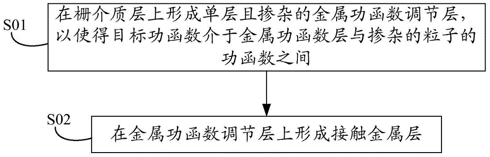
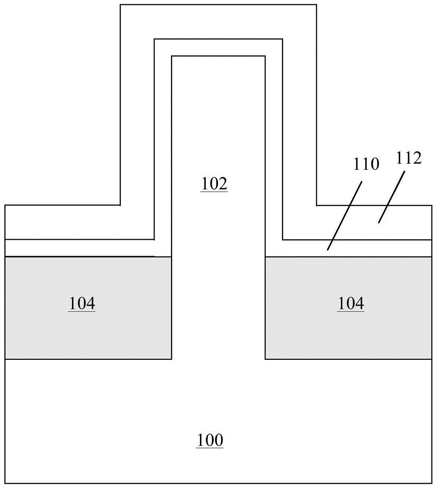
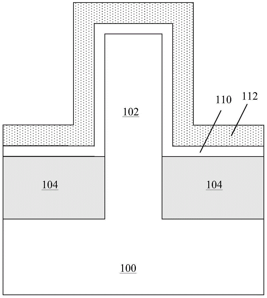
[0029] The present invention proposes a method for forming a gate, referring to figure 1 As shown, it includes: forming a single-layer metal work function adjustment layer on the gate dielectric layer; doping the metal work function adjustment layer so that the target work function is between the work function of the metal work function layer and the doped particles Between; forming a contact metal layer on the metal work function adjustment layer.

[0030] In the present invention, a single-layer metal work function adjustment layer is...


PUM


Abstract

The invention provides a gate forming method comprising the steps of forming a single doped metal work function adjustment layer on a gate dielectric layer to enable a target work function to be between the metal work function layer and a work function of doped particles, and forming other gate layers on the metal work function adjustment layer. Through the method, the threshold voltage can be adjusted easily, the process is simple and can be implemented without multiple metal gate layers, and the manufacturing cost is reduced.

Description

technical field [0001] The invention relates to the field of semiconductor devices, in particular to a gate and a forming method thereof. Background technique [0002] With the continuous reduction of device size, CMOS device gate engineering research centered on "high-k metal gate (high-k gate dielectric material and metal gate)" technology is the most representative core process in 22nm and below technologies . [0003] In the gate structure of a high-k metal gate, the threshold voltage Vt is adjusted through the work function of the metal gate, and in order to obtain a suitable threshold voltage, it is usually necessary to deposit multiple layers of different metal gate materials separately. The process is complex and not suitable for realization, especially for three-dimensional fin devices, it is even more difficult to realize. Contents of the invention [0004] The object of the present invention is to solve the above-mentioned technical defects, and provide a gate...

Claims


Application Information

Patent Timeline
Patent Type & Authority Applications(China)
IPC IPC(8): H01L29/10H01L21/28
Inventor 张青竹殷华湘闫江李俊峰杨涛刘金彪徐秋霞
Owner INST OF MICROELECTRONICS CHINESE ACAD OF SCI
Why Eureka
Try Eureka