A kind of organic thin film transistor and its preparation method

An organic thin film and transistor technology, applied in the field of organic thin film transistors and its preparation, can solve the problems of small voltage regulation range, complex surface modification process, unsatisfactory practical prospects, etc., and achieve the effect of simple process

Active Publication Date: 2022-05-31
湖南工商大学
View PDF4 Cites 0 Cited by
  • Summary
  • Abstract
  • Description
  • Claims
  • Application Information

AI Technical Summary

Problems solved by technology

There are many research works on how to effectively regulate the threshold voltage of organic thin film transistors, mainly focusing on the doping of organic semiconductors and modifying the surface of the insulating layer; but the difficulty lies in: doping and surface modification processes (such as surface coating alone Molecular layers, etc.) are complex, and it is difficult to effectively control the doping and surface modification of the insulating layer; the voltage regulation range is small, and precise regulation cannot be achieved
The above factors lead to the side effect of inappropriately changing the performance of the transistor in the process of adjusting the threshold voltage, which makes the practical prospect unsatisfactory.

Method used


Image

  • A kind of organic thin film transistor and its preparation method
  • A kind of organic thin film transistor and its preparation method
  • A kind of organic thin film transistor and its preparation method

Examples


Embodiment 1

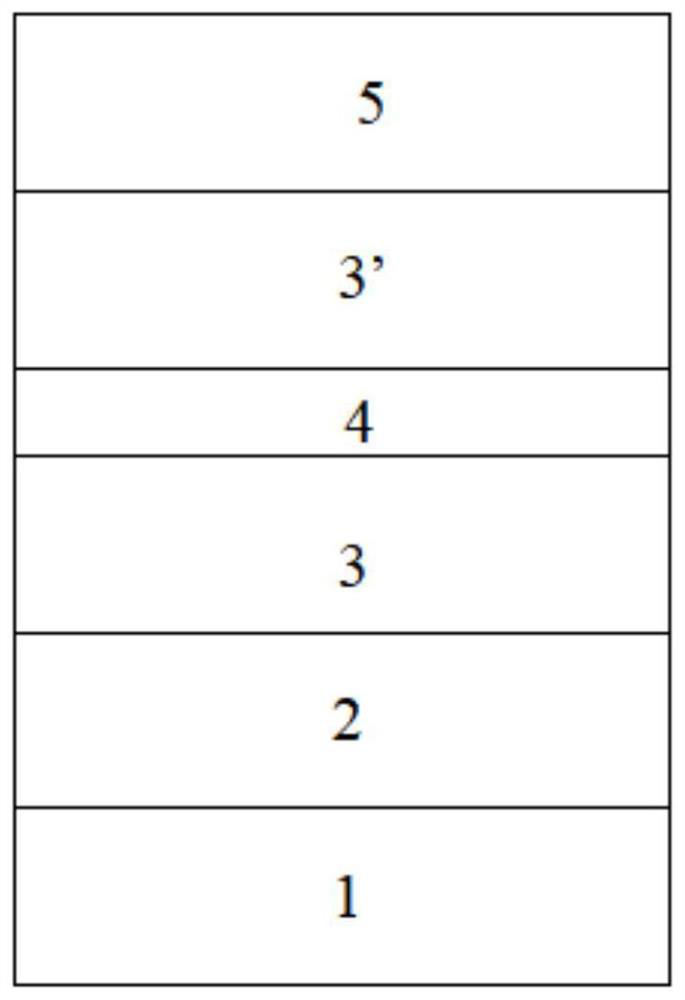
[0046] The mixed layer sequentially includes a semiconductor lower layer, a copper oxide layer and a semiconductor upper layer from bottom to top;

[0047] The semiconductor lower layer and the semiconductor upper layer are the same semiconductor material, both of which are pentacene.

[0049] S1. p-type silicon is taken to a specified thickness and used as a gate electrode.

Embodiment 2

[0056] The mixed layer sequentially includes a semiconductor lower layer, a copper oxide layer and a semiconductor upper layer from bottom to top;

[0057] The semiconductor lower layer and the semiconductor upper layer are the same semiconductor material, both of which are pentacene.

[0059] S1. Using a DC magnetron sputtering method, an aluminum film of a specified thickness is prepared for use as a gate electrode.

[0063] FIG. 1 shows a device structure diagram of the organic thin film transistor of the above-mentioned Embodiments 1-2. It can be seen from the figure that the oxygen


PUM

PropertyMeasurementUnit
thicknessaaaaaaaaaa
thicknessaaaaaaaaaa
currentaaaaaaaaaa

Abstract

The invention relates to an organic thin film transistor, which includes a mixed layer, wherein the mixed layer includes a semiconductor lower layer, a copper oxide layer and a semiconductor upper layer in order from bottom to top; the semiconductor lower layer and the semiconductor upper layer are the same or different semiconductor materials. The organic thin film transistor containing the copper oxide layer proposed by the invention can effectively adjust the threshold voltage of the organic thin film transistor. This regulation method does not need to rely on complex semiconductor doping and insulating layer surface modification technologies, and is a technology with simple processes and more suitable for commercial applications.

Description

A kind of organic thin film transistor and preparation method thereof technical field [0001] The invention belongs to the field of organic semiconductors, in particular to a kind of organic thin film transistor and preparation method thereof. Background technique Thin-film transistor is to use electric field to carry out control, realize current or voltage on and off, is to use changing external electric Active thin-film devices that control the conductivity of organic / inorganic semiconductor materials by field are also a class of components in driving circuits. With the development of organic electroluminescence (OLED) and liquid crystal flat panel display (LCD) technologies, in addition to the preparation of thin film crystals from silicon materials In addition to the tube, thin-film transistors (OTFTs) prepared with organic materials have also been developed. The main advantage is that organic materials have rich properties, Its properties are easily regulated by ...

Claims


Application Information

Patent Timeline
Patent Type & Authority Patents(China)
IPC IPC(8): H01L51/30H01L51/05H01L51/40B82Y30/00B82Y40/00
CPCB82Y30/00B82Y40/00H10K71/00H10K71/164H10K10/466H10K10/486H10K10/488H10K2102/00Y02P70/50
Inventor 聂国政李德琼陈智全许辉
Owner 湖南工商大学
Why Eureka
Try Eureka