Buried channel transistor and method of forming same

A transistor and channel technology, applied in the field of buried channel transistors and their formation, to prevent flicker noise and improve performance

Active Publication Date: 2020-10-30
SEMICONDUCTOR MANUFACTURING INTERNATIONAL (BEIJING) CORP +1
View PDF6 Cites 0 Cited by
  • Summary
  • Abstract
  • Description
  • Claims
  • Application Information

AI Technical Summary

Problems solved by technology

[0005] The problem that the present invention solves is how to prevent the generation of the flicker noise of existing transistor

Method used


Image

  • Buried channel transistor and method of forming same
  • Buried channel transistor and method of forming same
  • Buried channel transistor and method of forming same

Examples


Embodiment Construction

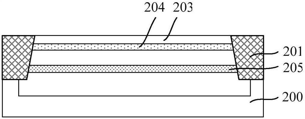
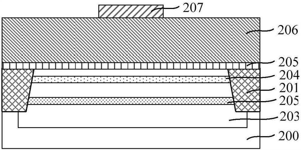
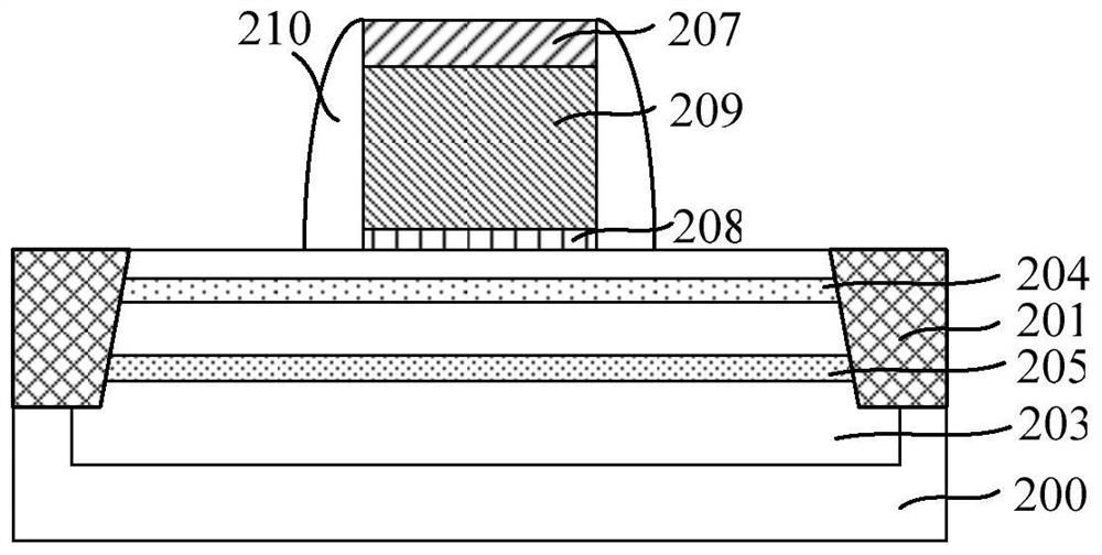
[0030] As mentioned in the background art, the performance of transistors formed in the prior art still needs to be improved. For example, the existing transistors have 1 / f noise or flicker noise during operation, and the generation of 1 / f noise or flicker noise is related to conduction. The smoothness of the channel has a great correlation, and the conductive channel formed by the existing transistor is basically a surface channel. In the manufacturing process, the smoothness of the substrate surface is difficult to ensure, and the substrate surface is inevitable. There will be defects, and the existence of defects will affect the transfer of carriers. Therefore, the existing transistors are prone to flicker noise during operation, which affects the performance of the device.

[0031] To this end, the present invention provides a buried channel transistor and a method for forming the same. By forming an inverse doped region in the well region, the carriers will travel along the g...


PUM


Abstract

A buried channel transistor and a forming method thereof, the forming method comprising: providing a semiconductor substrate, forming a well region in the semiconductor substrate; forming an inversion doped region in the well region, and in the inversion doped region The type of doping is opposite to the type of doping in the well region, and the depth of the inversion doped region is smaller than the depth of the well region; a gate structure is formed on the surface of the semiconductor substrate above the inversion doped region, so The gate structure includes a gate dielectric layer and a gate electrode located on the gate dielectric layer, the gate electrode is doped with impurity ions, and the type of doping in the gate electrode is the same as that of the well region; A source region and a drain region are formed in the semiconductor substrate on both sides of the pole structure. The doping type in the source region and the drain region is opposite to the impurity ion type in the well region. The depth of the source region and the drain region is smaller than the depth of the well region and Greater than the depth of the inversion doped region. The transistor formed by the method of the invention prevents the generation of flicker noise and improves the performance of the device.

Description

Technical field [0001] The invention relates to the field of semiconductor manufacturing, in particular to a buried channel transistor and a method for forming the same. Background technique [0002] Metal-oxide-semiconductor (MOS) transistors are the most basic devices in semiconductor manufacturing. They are widely used in various integrated circuits. They are divided into NMOS and PMOS transistors according to the main carriers and the type of doping during manufacturing. [0003] The prior art provides a method for manufacturing a MOS transistor. The method includes: providing a semiconductor substrate, forming an isolation structure on the semiconductor substrate, the semiconductor substrate between the isolation structures is an active region, and forming a well region (not shown) in the active region; Impurity ions are doped on the surface of the well region to adjust the threshold voltage of the subsequently formed transistor; a gate dielectric layer and a gate electrode a...

Claims


Application Information

Patent Timeline
Patent Type & Authority Patents(China)
IPC IPC(8): H01L29/78H01L21/336H01L29/06H01L29/423
CPCH01L29/0684H01L29/42372H01L29/66477H01L29/7838H01L21/823412H01L21/823418H01L21/82345H10B41/42H10B41/35H01L21/26513H01L21/266H01L21/32139H01L21/76224H01L21/823807H01L21/823814H01L21/823828H01L21/823864H01L21/823878H01L27/0922H01L29/04H01L29/0649H01L29/0688H01L29/0847H01L29/1033H01L29/1083H01L29/1095H01L29/1608H01L29/161H01L29/167H01L29/66825
Inventor 邱慈云克里夫·德劳利辜良智江宇雷余达强
Owner SEMICONDUCTOR MANUFACTURING INTERNATIONAL (BEIJING) CORP
Why Eureka
Try Eureka