Method for forming fin field effect transistor

A fin field effect and transistor technology, applied in semiconductor devices, semiconductor/solid-state device manufacturing, electrical components, etc., can solve problems such as difficult threshold voltage of fin field effect transistors

Active Publication Date: 2017-06-16
SEMICON MFG INT (SHANGHAI) CORP
View PDF1 Cites 0 Cited by
  • Summary
  • Abstract
  • Description
  • Claims
  • Application Information

AI Technical Summary

Problems solved by technology

[0005] However, with the continuous reduction in the size of FinFETs, it becomes more and more difficult to control the threshold voltage of FinFETs, especially the disturbance of dopant substances makes the above problems more prominent

Method used


Image

  • Method for forming fin field effect transistor
  • Method for forming fin field effect transistor
  • Method for forming fin field effect transistor

Examples


Embodiment Construction

[0023] In order to make the above objects, features and advantages of the present invention more comprehensible, specific implementations of the present invention will be described in detail below in conjunction with the accompanying drawings.

[0024] In the following description, many specific details are set forth in order to fully understand the present invention, but the present invention can also be implemented in other ways than those described here, so the present invention is not limited by the specific embodiments disclosed below.

[0025] As mentioned in the background section, as the size of FinFETs continues to decrease, it is difficult to control the threshold voltage of FinFETs formed in the prior art.

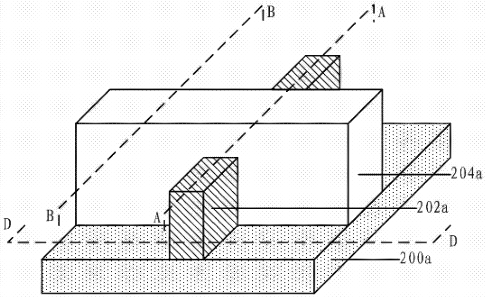
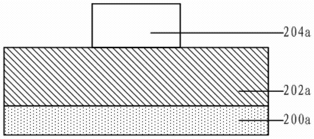
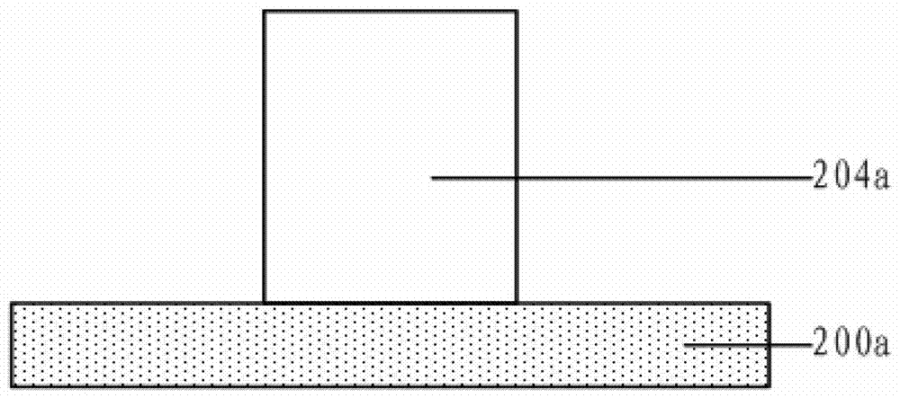
[0026] In view of the above defects, the present invention provides a method for forming a fin field effect transistor. Before forming the metal gate, the second sidewall and the fins above the second sidewall are respectively formed on the fins on both sides of ...


PUM


Abstract

A forming method of a fin type field effect transistor comprises the following steps: providing a semiconductor substrate having a fin portion and a dummy grid electrode crossing a top portion and a side wall of the fin portion; forming an interlayer medium layer on the fin portion on two sides of the dummy grid electrode and the semiconductor substrate, and a top surface of the interlayer medium layer is flush with a top surface of the dummy grid electrode; etching the dummy grid electrode until the dummy grid electrode with partial thickness is left on the top of the fin portion, thereby forming a first groove; forming a first side wall on a side wall of the first groove; using the first side wall as a mask to continuously etch the dummy grid electrode through anistropic etching technology until the semiconductor substrate is exposed, thereby forming a second groove; processing the remained dummy grid electrode so as to form a second side wall; forming a metal grid electrode in the second groove comprising the second side wall. The threshold-voltage of the fin type field effect transistor formed by the method can be controlled, and the formed fin type field effect transistor has better performance.

Description

technical field [0001] The invention relates to the technical field of semiconductor manufacturing, in particular to a method for forming a fin field effect transistor. Background technique [0002] In order to keep up with the pace of Moore's Law, people have to gradually shrink the feature size of a metal oxide semiconductor field effect transistor (MOSFET for short). Doing so can bring benefits such as increasing chip density and improving the switching speed of MOSFETs. However, as the channel length of the transistor is shortened, the distance between the drain and the source is also shortened, so that the control ability of the gate to the channel becomes worse, and the difficulty of pinching off the channel by the gate voltage is also reduced. It becomes larger and larger, so that the phenomenon of subthreshold leakage (Subthreshold leakage), that is, the so-called short-channel effects (short-channel effects, referred to as SCE) is more likely to occur. [0003] Fo...

Claims


Application Information

Patent Timeline
Patent Type & Authority Patents(China)
IPC IPC(8): H01L21/336
CPCH01L29/66545H01L29/66795
Inventor 张海洋李天慧舒强
Owner SEMICON MFG INT (SHANGHAI) CORP
Why Eureka
Try Eureka