Array test circuit and array test method

An array test and circuit technology, applied in the direction of static indicators, instruments, etc., can solve the problems of large layout space occupied by switches, large workload, and large number of signals, so as to reduce the number of input signals, save layout space, and improve flexibility sexual effect

Active Publication Date: 2019-04-05
WUHAN CHINA STAR OPTOELECTRONICS TECH CO LTD
View PDF6 Cites 0 Cited by
  • Summary
  • Abstract
  • Description
  • Claims
  • Application Information

AI Technical Summary

Problems solved by technology

[0004] The technical problem to be solved by the present invention is to provide an array test circuit and an array test method, which are used to solve the problem that the switches of the array test circuit in the prior art occupy a large layout space, and the design flexibility of the circuits around the panel is low, which is not conducive to narrow frame panels. Design, the number of input signals in array detection is large, and the workload is large, etc.

Method used


Image

  • Array test circuit and array test method
  • Array test circuit and array test method
  • Array test circuit and array test method

Examples


Embodiment Construction

[0026] The following will clearly and completely describe the technical solutions in the embodiments of the present invention with reference to the accompanying drawings in the embodiments of the present invention. Obviously, the described embodiments are only some, not all, embodiments of the present invention. Based on the embodiments of the present invention, all other embodiments obtained by persons of ordinary skill in the art without making creative efforts belong to the protection scope of the present invention.

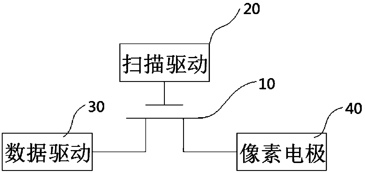
[0027] figure 1 The schematic diagram of the array substrate of the display state of the liquid crystal display provided in Embodiment 1 of the present invention, as shown in the figure, the gate of the thin film transistor 10 is connected to the scan driver 20, the drain of the thin film transistor 10 is connected to the data driver 30, and the source of the thin film transistor 10 is The pole is connected to the pixel electrode 40. In the display mode, the ...


PUM


Abstract

The invention discloses an array test circuit. The circuit comprises a scanning driver, an enablement driver, pixel control drivers, thin film transistors (TFTs) and pixel electrodes, the TFTs are positioned in a pixel unit of an array substrate, and is controlled, by a system driving circuit, to adjust the offset voltage of the pixel electrodes when display of a liquid crystal panel is normal, the grid electrodes of the TFTs are connected to the enablement driver, the enablement driver sends enablement signals and controls ON / OFF states of the TFTs simultaneously, the drain electrodes of the TFTs are connected to the scanning driver, the input end of each pixel control driver is connected to the source electrode of one TFT correspondingly, and the output end of each pixel control driver is connected to one pixel electrode correspondingly. According to the invention, a lot of layout space in the edge of the display panel is reduced, the amount of input signals during array test is small, and the array test process is simplified.

Description

technical field [0001] The invention relates to the field of display technology, in particular to an array test circuit and an array test method. Background technique [0002] Thin Film Transistor-LCD (Thin Film Transistor-LCD, TFT-LCD) has been developed rapidly and widely used in recent years. It is widely used in display devices of portable mobile electronic products, such as mobile phones, digital cameras, handheld computers, GPRS, etc. mobile products. A liquid crystal display panel is generally formed by pairing a color filter substrate and an array substrate, and a liquid crystal layer is encapsulated in the space between the two substrates. The array substrate mainly includes scanning lines, data lines and pixel electrodes. The scanning lines and the data lines are arranged vertically. The pixel electrodes are formed in the pixel area where the scanning lines and data lines are interlaced. The sent signal is sent to the corresponding pixel electrode through the thi...

Claims


Application Information

Patent Timeline
Patent Type & Authority Patents(China)
IPC IPC(8): G09G3/00G09G3/36
CPCG09G3/006G09G3/3648
Inventor 洪光辉龚强
Owner WUHAN CHINA STAR OPTOELECTRONICS TECH CO LTD
Why Eureka
Try Eureka