Array substrate, display panel and array substrate preparation method

A technology of array substrate and display area, which is applied in semiconductor/solid-state device manufacturing, electrical components, electric solid-state devices, etc. It can solve the problems of reflection, light leakage of metal leads in the surrounding lead area, and high production cost of narrow frame products, and achieve enhanced shading effect , Avoid reflections, reduce the effect of equipment investment

Inactive Publication Date: 2016-10-26
BOE TECH GRP CO LTD +1
View PDF5 Cites 13 Cited by
  • Summary
  • Abstract
  • Description
  • Claims
  • Application Information

AI Technical Summary

Problems solved by technology

[0006] Aiming at the above-mentioned deficiencies in the prior art, the present invention provides an array substrate, a display panel and a preparation method for the array substrate, which are used to at least partially solve the problems of high production cost of narrow frame products and light leakage and reflection of metal leads in the peripheral lead area.

Method used


Image

  • Array substrate, display panel and array substrate preparation method
  • Array substrate, display panel and array substrate preparation method

Examples


Embodiment 1

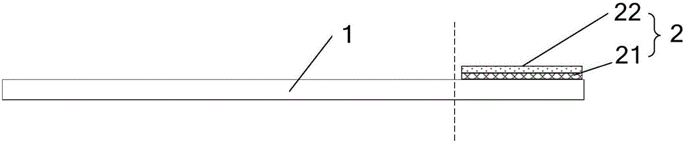
[0045] This embodiment provides an array substrate, such as figure 1 As shown, it includes a base 1. The base 1 includes a display area and a lead area. The display area is an area for forming thin film transistors, pixel electrodes, and common electrodes, including the thin film transistor area and the electrode area. The wire area is an area used to form metal wires connected to signal lines of thin film transistors, pixel electrodes, and common electrodes. The array substrate further includes a shielding layer 2, which is located in the wiring area of ​​the substrate 1 and is used to shield metal wirings (not shown in the figure) in the wiring area. The shielding layer 2 includes an anti-reflection film layer 21 , and the anti-reflection film layer 21 is formed on the substrate 1 .

[0046] Further, the shielding layer 2 may further include a metal film layer 22 , and the metal film layer 22 is formed on the anti-reflection film layer 21 . That is to say, the anti-reflect...

Embodiment 2

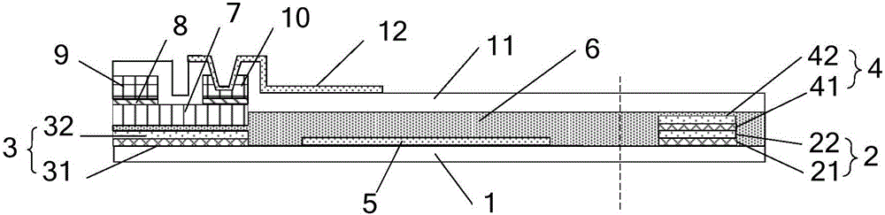
[0052] This embodiment provides an array substrate, such as figure 2 As shown, the difference between this embodiment and Embodiment 1 is that it also includes a first anti-reflection layer 3 formed on the substrate 1 in the display area. The reflectivity of metal film layers such as common electrodes and common electrodes to ambient light. The structure of the array substrate in embodiment 2 in the wiring area is the same as that in the array substrate in embodiment 1 in the wiring area, and will not be repeated here.

[0053]Specifically, the first anti-reflection layer 3 includes an anti-reflection film layer 31 and a metal film layer 32 , and the anti-reflection film layer 31 is located between the metal film layer 32 and the substrate 1 .

[0054] Further, such as figure 2 As shown, the array substrate may also include a second anti-reflection layer 4 formed on the shielding layer 2, the second anti-reflection layer 4 includes an anti-reflection film layer 41 and a me...

Embodiment 3

[0065] This embodiment provides a display panel. The display panel includes the aforementioned array substrate, and the structure of the array substrate will not be repeated here.

[0066] By forming a shielding layer in the lead region of the substrate, the shielding layer is used to shield the metal leads in the lead region, eliminating the exposed state of the metal wires in the lead region around the array substrate, avoiding the reflection of the metal leads, and being more beautiful; the anti-reflection film in the shielding layer The layer is located between the metal film layer and the substrate, which can reduce the reflectivity of external light, thereby enhancing the shading effect; in addition, the solution of the present invention can form a shading layer with the help of existing equipment in the array substrate preparation process, without additional ink coating Overlay equipment, reduce equipment investment, thereby reducing production costs.


PUM


Abstract

The invention provides an array substrate, a display panel and an array substrate preparation method. A shielding layer is formed in a lead wire area of a substrate, the shielding layer is utilized to shield metal lead wires in the lead wire area, the bared state of the metal lead wires in the lead wire area around the array substrate, light reflection of the metal lead wires is avoided, and the appearance is more beautiful; a reflection-reduction film layer in the shielding layer is arranged between a metal film layer and the substrate, and the reflection rate of external light is reduced, so that the light shielding effect is improved; in addition, the shielding layer can be formed by existing equipment in the array substrate preparation process, additional printing ink coating equipment is not needed, the equipment investment is reduced, and the production cost is lowered.

Description

technical field [0001] The invention relates to the field of display technology, in particular to an array substrate, a display panel and a method for preparing the array substrate. Background technique [0002] At present, in order to achieve a narrow frame or even a frameless design, it is necessary to place the array substrate on the light-emitting side of the display panel, and place the color filter substrate on the light-incoming side of the display panel, which can greatly narrow the connection pads for PCB bonding. The border of the region. [0003] However, in the peripheral lead area of ​​the array substrate, the metal leads are exposed. In order to shield the metal leads in the peripheral lead area of ​​the array substrate, the method of coating ink is usually used to cover at present. In this way, additional ink coating equipment and manpower are required. Material resources increase the production cost of products. [0004] In addition, due to the poor light-s...

Claims


Application Information

Patent Timeline
IPC IPC(8): H01L27/12H01L21/77
Inventor 王守坤郭会斌冯玉春李梁梁
Owner BOE TECH GRP CO LTD
Why Eureka
Try Eureka