
Packaging structure of DAF film-wrapped fingerprint sensor chip and manufacturing method of packaging structure

A sensor chip and packaging structure technology, which is applied in semiconductor/solid-state device manufacturing, instruments, electrical components, etc., can solve the problem of the need to pass through plastic packaging materials, cover plates or layers, large signal interference, packaging thickness chip surface and plastic packaging Problems such as the difficulty of controlling the body distance, etc., achieve the effect of saving the plastic sealing process, simplifying the process flow, and being easy to control

Inactive Publication Date: 2016-11-23
HUATIAN TECH XIAN
View PDF4 Cites 7 Cited by
  • Summary
  • Abstract
  • Description
  • Claims
  • Application Information

AI Technical Summary

Problems solved by technology

The surface of the fingerprint sensor chip is packaged with a plastic encapsulant, and the sensing signal needs to pass through the plastic encapsulant, cover or layer when collecting fingerprints, resulting in large signal interference, and it is difficult to control the thickness of the package and the distance between the chip surface and the plastic encapsulant

Method used


Image

  • Packaging structure of DAF film-wrapped fingerprint sensor chip and manufacturing method of packaging structure
  • Packaging structure of DAF film-wrapped fingerprint sensor chip and manufacturing method of packaging structure
  • Packaging structure of DAF film-wrapped fingerprint sensor chip and manufacturing method of packaging structure

Examples


Embodiment Construction

[0026] The present invention will be further described below in conjunction with accompanying drawing.

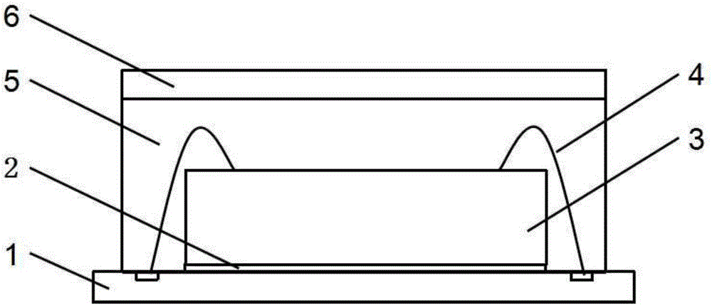
[0027] Such as figure 1 As shown, a packaging structure of a DAF film wrapped fingerprint sensor chip, including: a substrate 1, a fingerprint sensor chip 3, a protective cover 6, the fingerprint sensor chip 3 is located above the substrate 1, the fingerprint The pads of the sensor chip 3 face upward, and the fingerprint sensor chip 3 and the substrate 1 are interconnected by bonding wires 4, preferably two bonding wires 4, and the protective cover 6 is located on the Directly above the sensing area of ​​the fingerprint sensor chip 3 , the upper surface of the substrate 1 , the fingerprint sensor chip 3 , the bonding wire 4 and the lower surface of the protective cover 6 are wrapped by the DAF film 5 .

[0028] The DAF film 5 is in the form of a semi-solid adhesive film, which is viscous but does not flow. The DAF film 5 has high elasticity in a semi-solid state, and can ...


PUM


Abstract

The invention discloses a packaging structure of a DAF film-wrapped fingerprint sensor chip and a manufacturing method of the packaging structure. The packaging structure comprises a substrate, a fingerprint sensor chip and a protective cover plate, wherein the fingerprint sensor chip and the substrate are connected with each other by a bonding wire, and the upper surface of the substrate and the lower surfaces of the fingerprint sensor chip, the bonding wire and the protective cover plate are wrapped by DAF films. According to the packaging structure, the protective cover plate is directly pasted by adopting the DAF films, so that a plastic packaging procedure is omitted, and the process flow is simplified; additionally, the protective cover plate is directly pasted by adopting the DAF films, so that the spacing between the protective cover plate and the surface of the fingerprint sensor chip is easy to control, and the packaging structure is thin.

Description

technical field [0001] The invention relates to the technical field of sensor chip packaging, in particular to a packaging structure of a DAF film-wrapped fingerprint sensor chip and a manufacturing method thereof. Background technique [0002] With the progress of modern society, the importance of personal identification and personal information security has gradually attracted people's attention. Due to the uniqueness and invariance of human fingerprints, fingerprint identification technology has the characteristics of good security, high reliability, and simple and convenient use, making fingerprint identification technology widely used in various fields to protect personal information security, such as mobile phones, Various fingerprint identification systems have emerged in the fields of computers, access control, time attendance and other confidential systems. [0003] At present, sensor packages such as fingerprint readers, MEMS, optical sensors, and pressure sensors...

Claims


Application Information

Patent Timeline
Patent Type & Authority Applications(China)
IPC IPC(8): H01L23/31H01L21/56G06K9/00
CPCH01L21/56H01L23/3107G06V40/13H01L2224/48091H01L2224/73265H01L2924/00014
Inventor 安强
Owner HUATIAN TECH XIAN
Learn More