Shielding film and pasting method therefor
A technology of shielding film and film layer, applied in the bonding method of surface pretreatment, magnetic field/electric field shielding, electrical components, etc., can solve the problems of waste generation, waste of raw materials, etc., to reduce waste, improve paste efficiency, save The effect of raw materials
- Summary
- Abstract
- Description
- Claims
- Application Information
AI Technical Summary
Problems solved by technology
Method used
Image
Examples
Embodiment 1
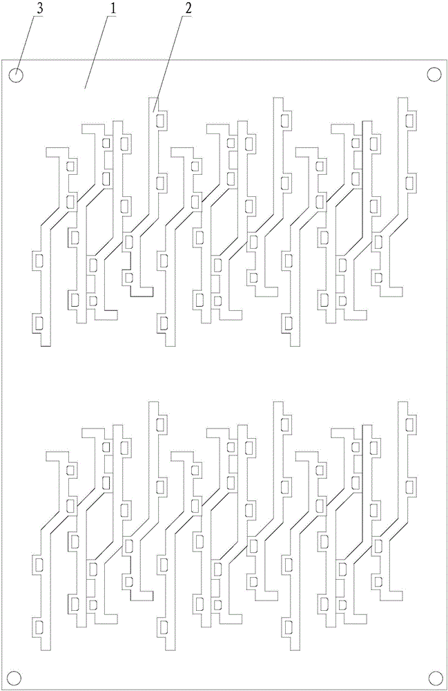
[0030] Please refer to figure 1 , Embodiment 1 of the present invention is:
[0031] A method for pasting a shielding film. The adhesive film 1 is punched. The adhesive film 1 includes a film layer and an adhesive layer, the adhesive layer is arranged on the film layer, and the adhesive layer is silica gel. The through hole 3 obtained after the adhesive film 1 is punched can be used as a mark and a positioning reference, and the viscosity of the adhesive film 1 is 0.5kgF / cm; the protective film on the shielding film is surface treated to increase the roughness of the protective film surface , so that the adhesive film 1 is closely connected with the protective film on the shielding film, it is convenient to remove the protective film on the shielding film when the adhesive film 1 is removed. The surface roughness Ra of the protective film is 1-3um, and Rz is 3 -5um.
[0032] The shielding film is punched to form a shielding film unit 2, the number of the shielding film unit ...
PUM
 Abstract
Description
Claims
Application Information
