Unlock instant, AI-driven research and patent intelligence for your innovation.

Data writing method, memory control circuit unit and memory storage device

A technology for writing data and controlling circuits, which is applied in the direction of electrical digital data processing, instruments, input/output to record carriers, etc., and can solve problems such as short service life, slow writing or erasing speed, and rapid decline in service life. To achieve the effect of avoiding the rapid decline of life expectancy

Active Publication Date: 2019-03-05
PHISON ELECTRONICS
View PDF8 Cites 0 Cited by
  • Summary
  • Abstract
  • Description
  • Claims
  • Application Information

AI Technical Summary

Problems solved by technology

However, compared with the physical erasing unit operating in the single-page mode, the service life of the physical erasing unit operating in the multi-page mode is relatively short, and corresponding to the writing of the physical erasing unit operating in the multi-page mode The critical value of the number of times of writing or erasing will be lower than the critical value of the number of times of writing or erasing corresponding to the physical erasing unit operating in the single page mode, and the writing or erasing of the physical erasing unit operating in the multi-page mode The erasing speed is also slower than the writing or erasing speed of the physical erasing unit operating in single page mode
[0008] Based on the above, how to avoid the rapid decline in the service life of the physical erasing unit operated in the multi-page mode, and how to improve the reliability and access speed of the flash memory in which each memory unit can store multiple bits is a technology in the art people's goals

Method used


Image

  • Data writing method, memory control circuit unit and memory storage device
  • Data writing method, memory control circuit unit and memory storage device
  • Data writing method, memory control circuit unit and memory storage device

Examples


Embodiment Construction

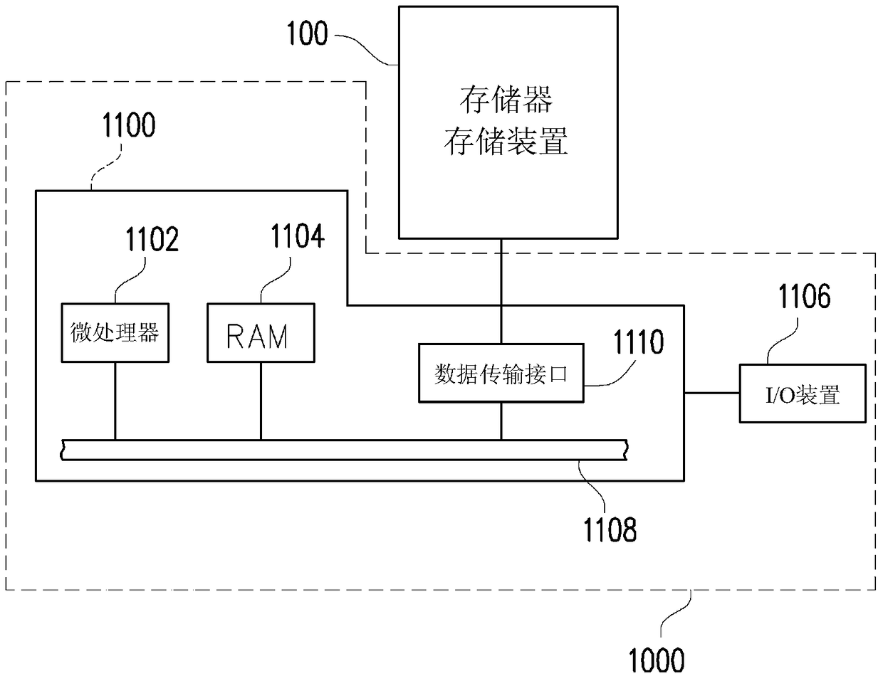
[0085] Figure 1A It is a schematic diagram of a host system and a memory storage device shown in an embodiment of the present invention. Figure 1B It is a schematic diagram of a computer, an input / output device and a memory storage device according to an embodiment of the present invention. Figure 1C It is a schematic diagram of a host system and a memory storage device shown in an embodiment of the present invention.

[0086] Please refer to Figure 1A , the host system 1000 generally includes a computer 1100 and an input / output (input / output, I / O for short) device 1106 . The computer 1100 includes a microprocessor 1102 , a random access memory (random access memory, RAM for short) 1104 , a system bus 1108 and a data transmission interface 1110 . The input / output device 1106 includes such as Figure 1B mouse 1202, keyboard 1204, monitor 1206 and printer 1208. It is important to understand that Figure 1B The devices shown are not limited to the input / output device 1106...


PUM


Abstract

The invention discloses a data write-in method, a memory control circuit unit and a memory storage device. The method comprises the following steps of: at least grouping entity erasing units into a temporary storage area and a storage area, selecting a first entity erasing unit in the temporary storage area, copying a plurality of effective data in the first entity erasing unit to a second entity erasing unit in the temporary storage area, and carrying out an erasing operation on the first entity erasing unit; and selecting a third entity erasing unit from the temporary storage area, copying a plurality of effective data in the third entity erasing unit to a fourth entity erasing unit of the storage area, and carrying out an erasing operation on the third entity erasing unit. According to the method, the service life of flash memories can be prolonged and the data access speed can be improved.

Description

technical field [0001] The present invention relates to a data writing method, and in particular to a data writing method for a rewritable non-volatile memory module, a memory controller and a memory storage device. Background technique [0002] The rapid growth of digital cameras, mobile phones, and MP3 players has led to a rapid increase in consumer demand for storage media. Because rewritable non-volatile memory (rewritable non-volatile memory) has the characteristics of data non-volatility, power saving, small size, no mechanical structure, fast read and write speed, etc., it is most suitable for portable electronic products, such as notebook computers . A solid state drive is a memory storage device that uses flash memory as a storage medium. Therefore, the flash memory industry has become a very popular part of the electronics industry in recent years. [0003] According to the number of bits that can be stored in each storage unit, NAND flash memory can be divided ...

Claims


Application Information

Patent Timeline
Patent Type & Authority Patents(China)
IPC IPC(8): G06F13/16G06F3/06
Inventor 叶志刚
Owner PHISON ELECTRONICS