Unlock instant, AI-driven research and patent intelligence for your innovation.

Transmission electron microscope sample stage loading area with field effect transistor function

A technology for transmission electron microscope samples and field effect transistors, which is applied in circuits, discharge tubes, electrical components, etc., can solve problems such as the inability to provide the working environment of field effect transistors, the exploration of structural changes and structure-performance relationships, and the inability to use transmission electron microscopes.

Active Publication Date: 2016-12-07
TIANJIN UNIVERSITY OF TECHNOLOGY
View PDF17 Cites 3 Cited by
  • Summary
  • Abstract
  • Description
  • Claims
  • Application Information

AI Technical Summary

Problems solved by technology

But for field effect transistor materials, this kind of sample loading area and the aforementioned other sample loading areas and sample stages cannot provide electric field effects to create a transistor working environment, so it is impossible to use transmission electron microscopy to explore the structural changes of this type of material in the transistor working environment and structure-performance relationship

Method used


Image

  • Transmission electron microscope sample stage loading area with field effect transistor function
  • Transmission electron microscope sample stage loading area with field effect transistor function
  • Transmission electron microscope sample stage loading area with field effect transistor function

Examples


Embodiment 1

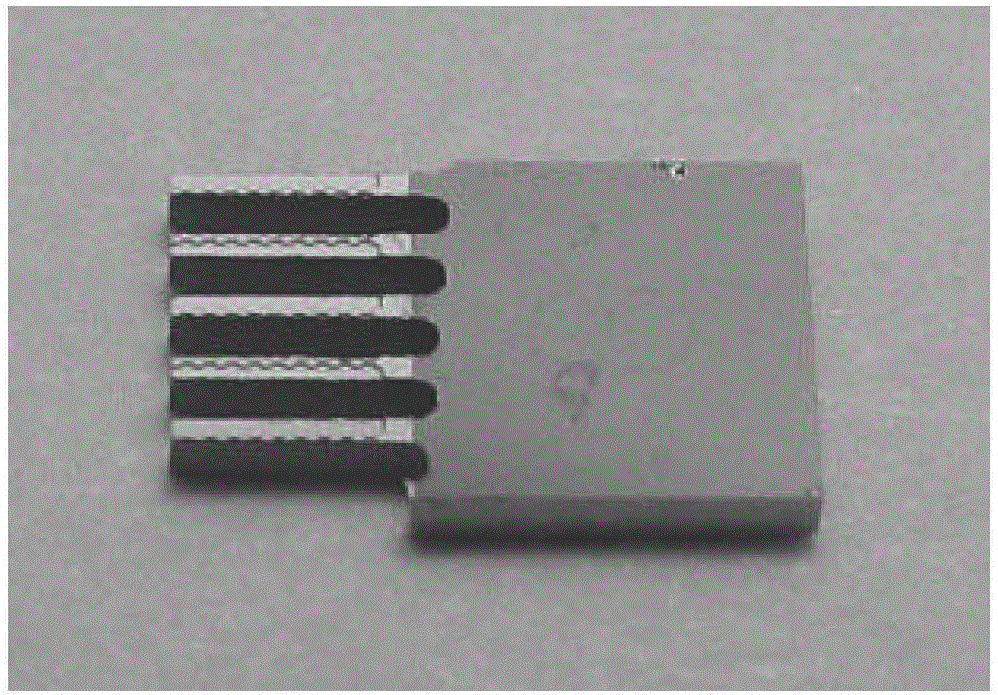
[0031] Preparation of the sample loading area of ​​the transmission electron microscope sample stage with the function of field effect transistor based on the size of 10mmX10mm, Pt electrodes, and 5 probes:

[0032] Clean the surface of the Si substrate with a 98% alcohol solution, blow it off with high-purity nitrogen, and grow a layer of SiO with a thickness of 80nm on the surface by heating and growing. 2 insulating layer, formed covered with SiO 2 Si sheet substrate with oxide layer; SiO 2 The insulating layer is etched into the same pattern as the final electrode shape, wherein the distance between the source pattern and the drain pattern is 2 μm; the gaps and gaps between the source pattern, the drain pattern and the gate pattern are etched; Deposit Pt electrodes on the source pattern, the drain pattern and the gate pattern, as the three electrodes of the source, the drain and the gate; use a diamond saw to cut the sample-loading region into probes, and obtain the follo...

Embodiment 2

[0035] The preparation of the sample loading area of ​​the transmission electron microscope sample stage with the function of field effect transistor based on the size of 5mmX5mm, Cu electrode, and 3 probes:

[0036] Clean the surface of the Si substrate with a 98% alcohol solution, blow it off with high-purity nitrogen, and grow a layer of SiO with a thickness of 70nm on the surface by heating and growing. 2 insulating layer, formed covered with SiO 2 Si sheet substrate with oxide layer; SiO 2 The insulating layer is etched into the same pattern as the final electrode shape, wherein the distance between the source pattern and the drain pattern is 6 μm; the gaps and gaps between the source pattern, the drain pattern and the gate pattern are etched; Deposit Cu electrodes on the source pattern, drain pattern, and gate pattern as the three electrodes of source, drain, and gate; use a diamond saw to cut the sample loading area into 3 probes, each probe There are multiple field-e...

Embodiment 3

[0038] Preparation of the sample loading area of ​​the TEM sample stage with the function of field effect transistor based on the size of 6mmX6mm, Au electrodes, and 4 probes:

[0039] Clean the surface of the Si substrate with a 98% alcohol solution, blow it off with high-purity nitrogen, and grow a layer of SiO with a thickness of 60 nm on the surface by heating and growing. 2 insulating layer, formed covered with SiO 2 Si sheet substrate with oxide layer; SiO 2 The insulating layer is etched into the same pattern as the final electrode shape, wherein the distance between the source pattern and the drain pattern is 8 μm; the gaps and gaps between the source pattern, the drain pattern and the gate pattern are etched; Deposit Au electrodes on the source pattern, drain pattern and gate pattern as the three electrodes of source, drain and gate; use a diamond saw to cut the sample loading area into 4 probes, each probe There are multiple field-effect transistor structures; the ...


PUM


Abstract

The invention provides a transmission electron microscope sample stage loading area with a field effect transistor function. The transmission electron microscope sample stage loading area comprises a probe area and a blank area, wherein the blank area is not provided with a transistor and is only covered with an Si substrate which takes SiO2 as an insulating layer; the probe area comprises at least one probe; each probe comprises at least one field effect transistor which is sequentially arranged; each field effect transistor covers the surface of an Si substrate layer by employing Si as a substrate material and the SiO2 as the insulating layer; a gate G is located at the center of the bottom part of the Si substrate layer, a source S and a drain D are located at the upper part of the SiO2 insulating layer, and a channel region is arranged between the source S and the drain D; and a to-be-characterized sample is put into the channel region. The transmission electron microscope sample stage loading area has the advantages that a material sample suitable for characterization can be a semiconductor material, and can also be a conductive material or an insulating material, and can form a closed loop in the transistor; real-time characterization of electrical properties and a structure change is achieved; and a new method is provided for analyzing the relationship between the structure and the electrical properties of the test material.

Description

technical field [0001] The invention belongs to the technical field of electron microscopy characterization of functional materials, in particular to a sample-carrying area of ​​a transmission electron microscope sample stage with the function of a field-effect transistor and a preparation method thereof. Background technique [0002] Transmission electron microscopy is an advanced technology that uses electron beams as light sources and electromagnetic fields as lenses to characterize the surface and internal structure of materials. There are many kinds of materials that can be characterized by transmission electron microscopy, including metal materials, non-metal materials, powder particles as small as tens of nanometers, thin films with a thickness of only a few nanometers, and biological materials. Transmission electron microscopy technology provides the possibility to explore the structural information of these materials, reveal the structure regulation mechanism of the...

Claims


Application Information

Patent Timeline
Patent Type & Authority Applications(China)
IPC IPC(8): H01J37/20
CPCH01J37/20
Inventor 罗俊刘锐锐
Owner TIANJIN UNIVERSITY OF TECHNOLOGY
Features
  • R&D
  • Intellectual Property
  • Life Sciences
  • Materials
  • Tech Scout
  • Unparalleled Data Quality
  • Higher Quality Content
  • 60% Fewer Hallucinations
Learn More