Wireless charging receiving coil and preparation method thereof
A wireless charging and receiving coil technology, applied in the direction of transformer/inductor coil/winding/connection, circuit, inductor, etc., can solve the problems of difficult integration and large area, and achieve high power receiving ability and high quality factor. Effect
- Summary
- Abstract
- Description
- Claims
- Application Information
AI Technical Summary
Problems solved by technology
Method used
Image
Examples
Embodiment 1
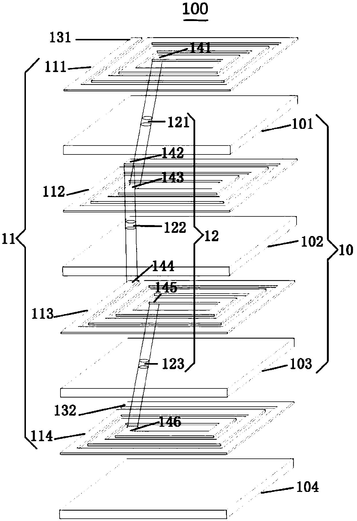
[0086] see figure 1 Shown is the structure of a wireless charging receiving coil provided in Embodiment 1 of the present application. The wireless charging receiving coil is a 4-layer series structure, including 1 layer of flexible substrate 104, 3 flexible insulating layers 10, and 4 conductive coil layers. 11, 3 via holes 12, 2 terminals 131, 132. The bottom layer is the flexible substrate 104 as the base layer, and the upward sequence is the first conductive coil layer 114, the first insulating layer 103, the second conductive coil layer 113, the second insulating layer 102... until the fourth conductive coil layer The coil layers 111 are separated by insulating layers 10 between adjacent conductive coil layers, forming a multi-layer structure in which conductive coil layers and insulating layers are stacked alternately.
[0087] Wherein, the conductive coil layers of different layers have the same orientation after being connected in series, and the inner end 146 of the f...
Embodiment 2
[0095] see Figure 4 Shown is the structure of a wireless charging receiving coil provided by Embodiment 2 of the present application. The wireless charging receiving coil is a 4-layer series-parallel structure, in which the upper two layers 211, 212 are connected in parallel, and the lower two layers 213, 214 are connected in parallel. , and then the upper two layers are connected in series with the lower two layers, which also includes 1 layer of flexible substrate 204 , 3 flexible insulating layers 20 , 4 conductive coil layers 21 , 5 via holes 22 , and 2 terminals 231 , 232 . The bottom layer is the base layer 204, and upwards are the first conductive coil layer 214, the first insulating layer 203, the second conductive coil layer 213, the second insulating layer 202... until the fourth conductive coil layer 211, Adjacent conductive coil layers are separated by insulating layers 20 to form a multi-layer structure in which conductive coils and insulating layers are stacked ...
PUM
| Property | Measurement | Unit |
|---|---|---|
| thickness | aaaaa | aaaaa |
| length | aaaaa | aaaaa |
| width | aaaaa | aaaaa |
Abstract
Description
Claims
Application Information


