Fingerprint identification display panel, production method thereof, driving method thereof, and display device

A display panel, fingerprint recognition technology, applied in static indicators, character and pattern recognition, acquisition/organization of fingerprints/palmprints, etc., can solve the mutual interference between fingerprint recognition detection signals and display signals, and affect the quality of fingerprint recognition question

Active Publication Date: 2016-12-21
BOE TECH GRP CO LTD
View PDF6 Cites 48 Cited by
  • Summary
  • Abstract
  • Description
  • Claims
  • Application Information

AI Technical Summary

Problems solved by technology

At present, fingerprint recognition display panels generally adopt capacitive structure to realize the function of fingerprint recognition. For example, in-cell fingerprint recognition display Fingerprint identification components are easy to generate parasitic capacitance with the components inside the display panel, which makes the fingerprint identification detection signal and display signal interfere with each other, thus affecting the quality of fingerprint identification

Method used


Image

  • Fingerprint identification display panel, production method thereof, driving method thereof, and display device
  • Fingerprint identification display panel, production method thereof, driving method thereof, and display device
  • Fingerprint identification display panel, production method thereof, driving method thereof, and display device

Examples


Embodiment Construction

[0033] The specific implementations of the fingerprint identification display panel, its manufacturing method, its driving method and display device provided by the embodiments of the present invention will be described in detail below with reference to the accompanying drawings.

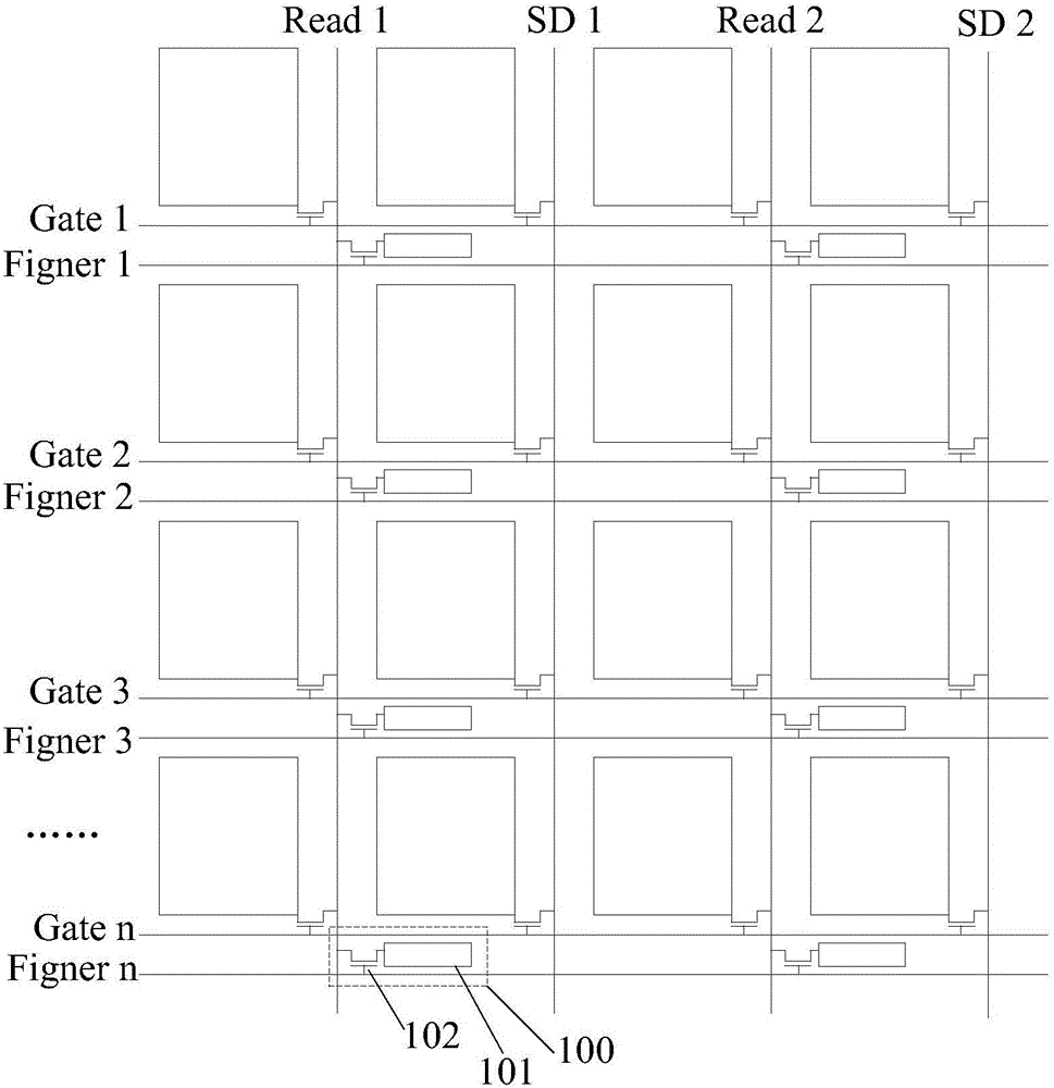
[0034] An embodiment of the present invention provides a fingerprint identification display device, such as figure 1 As shown, it includes: a plurality of ultrasonic detection units 100 arranged in an array arranged inside the display device, a plurality of identification scanning lines Finger 1 to n, and a plurality of identification output lines Read 1 and 2; wherein,

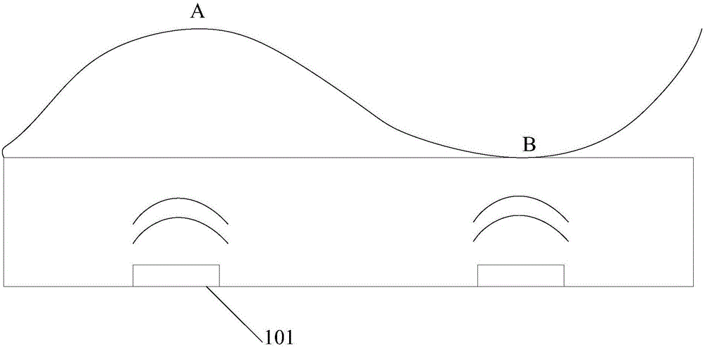
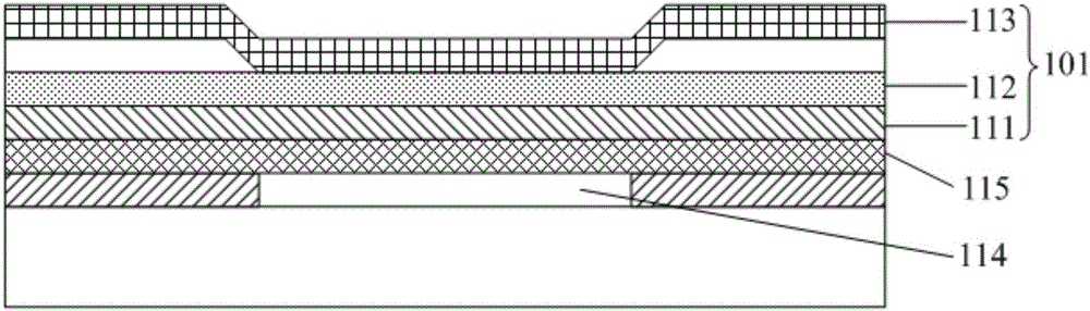
[0035] Each ultrasonic detection unit 100 includes: a pressure sensing unit 101 for generating ultrasonic waves and sensing ultrasonic changes brought about by fingerprint pressing, and a control switching transistor 102 for controlling the pressure sensing unit 101 to convert ultrasonic changes into different signal outputs ;

[...


PUM


Abstract

The invention discloses a fingerprint identification display panel, a production method thereof, a driving method thereof, and a display device. A plurality of ultrasonic wave detection units, a plurality of identification scanning lines, and a plurality of identification output lines are disposed in the display device. Every ultrasonic wave detection unit comprises a pressure-sensing unit used for generating ultrasonic waves and sensing the changes of the ultrasonic waves caused by pressing of fingerprints, and a control switch transistor used for controlling the pressure-sensing unit to convert the changes of the ultrasonic waves into different signals for output. When fingers of users are close to the surface of the display device, because of the uneven ridges and the uneven valleys of the skins of the fingers, the intensities of the ultrasonic waves transmitted by the pressure-sensing units reflected by the positions of the ridges and the valleys of the fingers back to the pressure-sensing units are different, and then the differences of the current signals converted by the pressure-sensing units are caused, and therefore the detection of the fingerprints is realized. The pressure-sensing unit is used for the detection of the fingerprints based on piezoelectric effect, and interferences on the internal parts in the display device are not easy to generate, and therefore high-quality fingerprint detection is easily realized.

Description

technical field [0001] The invention relates to the field of liquid crystal modules, in particular to a fingerprint recognition display panel, a manufacturing method thereof, a driving method thereof and a display device. Background technique [0002] With the rapid development of display technology, display panels with a fingerprint recognition function have gradually spread in people's lives. At present, fingerprint recognition display panels generally adopt capacitive structure to realize the function of fingerprint recognition. For example, in-cell fingerprint recognition display The fingerprint identification component is likely to generate parasitic capacitance with the components inside the display panel, so that the fingerprint identification detection signal and the display signal interfere with each other, thereby affecting the quality of fingerprint identification. Contents of the invention [0003] In view of this, the embodiments of the present invention prov...

Claims


Application Information

Patent Timeline
Patent Type & Authority Applications(China)
IPC IPC(8): G06K9/00G09G3/36
CPCG09G3/36G06V40/1306
Inventor 刘英明董学吕敬王海生陈小川吴俊纬丁小梁许睿赵利军李昌峰贾亚楠杨盛际郭玉珍刘伟王鹏鹏
Owner BOE TECH GRP CO LTD
Why Eureka
Try Eureka