Laser etching method and device, substrate electrode and electroluminescent device

A laser etching method and substrate electrode technology are applied in semiconductor devices, laser welding equipment, circuits, etc., and can solve problems such as lighting, adverse effects on device performance, and device leakage.

Active Publication Date: 2019-08-23
NANJING TECH CORP LTD
View PDF7 Cites 0 Cited by
  • Summary
  • Abstract
  • Description
  • Claims
  • Application Information

AI Technical Summary

Problems solved by technology

However, in the current laser etching process, the phenomenon of edge deposition often occurs, and the conductive material will be re-deposited on the edge of the area to be etched, forming a protrusion that is tens or even hundreds of nanometers higher than the original surface of the conductive material.
[0005] This kind of protrusion existing in the space corresponding to the edge of the area to be etched is likely to cause adverse effects on the performance of the device. In addition, during the preparation of thin-film devices, uneven film formation will be caused by edge protrusions; during the use of devices, a large amount of current will be gathered at the tip discharge, making the place The current density of the conductive material is higher than that of the flat part of the conductive material, which causes the phenomenon that the raised part of the edge is turned on before the internal area of ​​the device during the lighting process of the device

Method used


Image

  • Laser etching method and device, substrate electrode and electroluminescent device
  • Laser etching method and device, substrate electrode and electroluminescent device
  • Laser etching method and device, substrate electrode and electroluminescent device

Examples


Embodiment 1

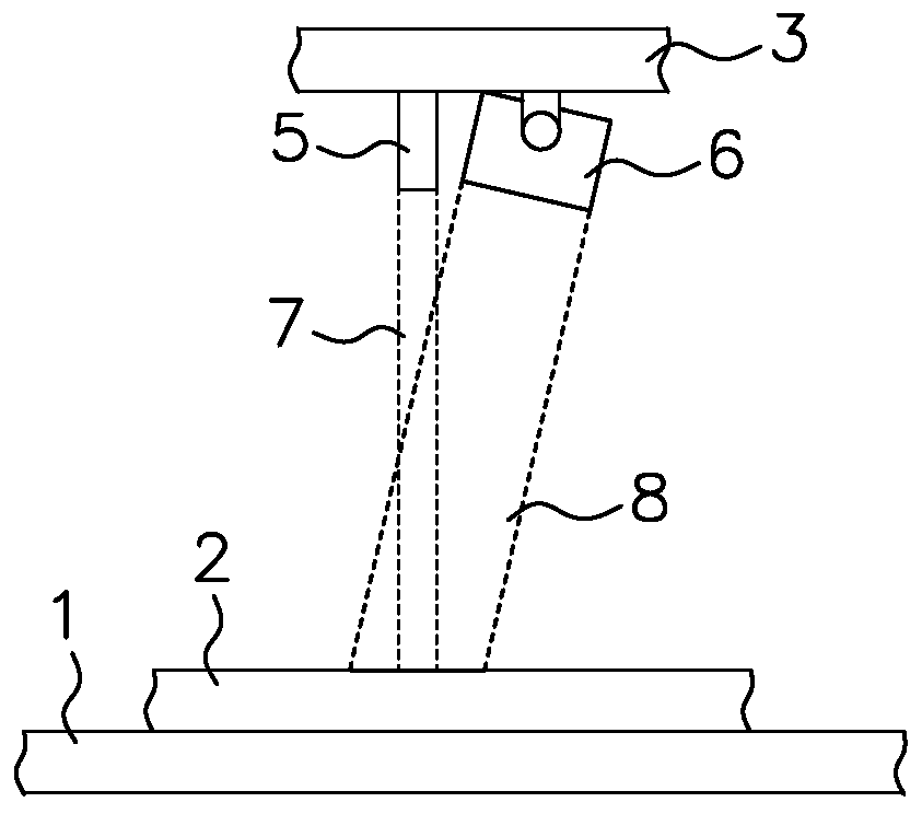
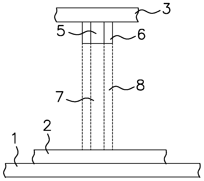
[0056] Such as figure 1 As shown, a kind of laser engraving machine that this embodiment provides, comprises the working platform 1 that is used to fix the object to be etched, and is arranged on the support 3 above the working platform 1, and the laser (comprising main laser 5) is installed on the support 3 and auxiliary laser 6), relative movement can occur between the working platform 1 and the support 3, and the relative movement can be in the horizontal direction or in the vertical direction.

[0057] The object to be etched includes a substrate coated with a conductive material. On the side coated with the conductive material, at least one region to be etched is provided on the object to be etched.

[0058] In this embodiment, the laser includes a main laser and an auxiliary laser.

[0059] Such as figure 2 show, combine figure 1 It can be seen that corresponding to one main laser 5, there may be one auxiliary laser 6. The main laser 5 is used to emit the main lase...

Embodiment 2

[0072] Such as Figure 12 As shown, a laser etching machine provided in this embodiment includes a working platform 1 for fixing the object to be etched, and a laser 4 arranged above the working platform 1, and a relative relationship between the working platform 1 and the laser 4 can occur. The relative movement can be horizontal or vertical.

[0073] The object to be etched 2 includes a substrate coated with a conductive material. On the side coated with the conductive material, at least one region to be etched is provided on the object to be etched.

[0074] Depend on Figure 12 and Figure 13 It can be seen that between the working platform 1 and the laser 4, the laser etching machine of this embodiment is also provided with an optical device for dividing the initial laser beam emitted by the laser into a main laser beam and an auxiliary laser beam.

[0075] Such as Figure 12 As shown, the optical device includes a total reflection mirror 12 having a through hole, an...

Embodiment 3

[0080] Take the ITO substrate as the object to be etched as an example, and use the laser etching machine in Embodiment 1 to etch it. The laser etching method includes:

[0081] (1) The front side of the ITO substrate to be etched (that is, the side provided with the ITO conductive material) is placed on the working platform of the laser etching machine and positioned;

[0082] (2) Adjust the distance between the working platform and the support, move the main laser to the top of the first area to be etched, so that the focus of the main laser beam falls on the first area to be etched;

[0083] (4) Input or import the ITO pattern to be etched into laser engraving software;

[0084] (5) Adjust the tilt angle of the auxiliary laser (when using figure 1 and Figure 8 The shown laser etching machine needs to adjust the tilt angle of the auxiliary laser, when using image 3 Not required for the laser engraving machine shown), adjust the beam size of the main laser beam and the a...


PUM


Abstract

The invention discloses a laser etching method and device, a substrate electrode and an electroluminescent device. The laser etching method comprises a step of etching an object to be etched by laser beams, wherein the object to be etched is provided with at least one region to be etched, and the laser beams include a main laser beam for gasifying a conducting material in the region to be etched and auxiliary laser beams for lowering the temperature falling rate in a space corresponding to the edge of the region to be etched. Two types of laser beams are adopted in the etching step: the main laser beam can gasify the conducting material in the region to be etched while the auxiliary laser beams are used for raising the temperature in the space corresponding to the edge of the region to be etched, so that the temperature falling rate in the space corresponding to the edge of the region to be etched is lowered, the gasified conducting material is prevented from being deposited due to over low temperature in the space corresponding to the edge of the region to be etched during outward diffusion of the gasified conducting material from the space corresponding to the region to be etched, and the formation of bumps on the surface of the object to be etched is avoided.

Description

technical field [0001] The invention belongs to the technical field of semiconductors, and in particular relates to a laser etching method and device, a substrate electrode and an electroluminescence device. Background technique [0002] The basic principle of laser etching is to focus a low-power laser beam with high beam quality (usually ultraviolet laser, fiber laser) into a very small spot, and form a high power density at the focus, so that the material is vaporized and evaporated in an instant, forming Holes, slots, slots. [0003] Laser etching utilizes the superior processing performance of laser, such as non-contact processing, high degree of flexibility, fast processing speed, no noise, small heat-affected zone, and extremely small spot that can be focused to the laser wavelength level, and can obtain good dimensional accuracy And processing quality, especially the interaction with certain materials (such as polyimide) is a "cold processing" of "photochemical acti...

Claims


Application Information

Patent Timeline
Patent Type & Authority Patents(China)
IPC IPC(8): B23K26/06B23K26/362B23K26/067B23K26/064B23K101/40
CPCB23K26/0608B23K26/064B23K26/0643B23K26/0676B23K26/361B23K2101/40
Inventor 陈超
Owner NANJING TECH CORP LTD
Why Eureka
Try Eureka