Touch display module and manufacture method thereof
A technology of touch display and manufacturing method, which is applied in optics, instruments, electrical digital data processing, etc., can solve the problems of high cost and increased thickness, and achieve the effects of low cost, improved performance, and obvious cost advantages
- Summary
- Abstract
- Description
- Claims
- Application Information
AI Technical Summary
Problems solved by technology
Method used
Image
Examples
Embodiment
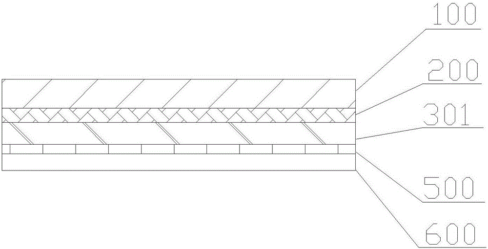
[0035] A touch display module, such as image 3 As shown, it includes a cover plate 100 , an optically transparent adhesive layer 200 , a touch function layer 301 with anti-glare and anti-reflection, foam glue 500 and a liquid crystal display layer 600 , and the cover plate 1 can optionally have a decorative layer.
[0036] In this embodiment, the product is set as a white touch display module, and its preparation method is as follows:
[0037] (1) The strengthened silicate glass is selected as the transparent substrate, the strengthening depth is 8 μm, and the spectral transmittance at a wavelength of 550 nm is greater than 91%;
[0038] (2) Transparent substrate cleaning;
[0039] (3) Print the white ink onto the transparent substrate by screen printing to form the cover plate 100 .
[0040] (4) Select a film with anti-glare and anti-reflection functions as the substrate, paste the transparent conductive material on the substrate, and form the pattern area of the functio...
PUM
| Property | Measurement | Unit |
|---|---|---|
| Square resistance | aaaaa | aaaaa |
Abstract
Description
Claims
Application Information


