Induction device used for detecting touching of user

A technology for sensing devices and sensing elements, applied in instruments, character and pattern recognition, print image acquisition, etc., can solve the problems of limited hardware configuration and process selection flexibility, so as to improve the possibility and flexibility of hardware configuration, avoid inconvenience, The effect of reducing the number

Inactive Publication Date: 2017-01-04
MSTAR SEMICON INC
View PDF2 Cites 4 Cited by
  • Summary
  • Abstract
  • Description
  • Claims
  • Application Information

AI Technical Summary

Problems solved by technology

However, this unavoidable packaging method considerably limits

Method used


Image

  • Induction device used for detecting touching of user
  • Induction device used for detecting touching of user
  • Induction device used for detecting touching of user

Examples


Example Embodiment

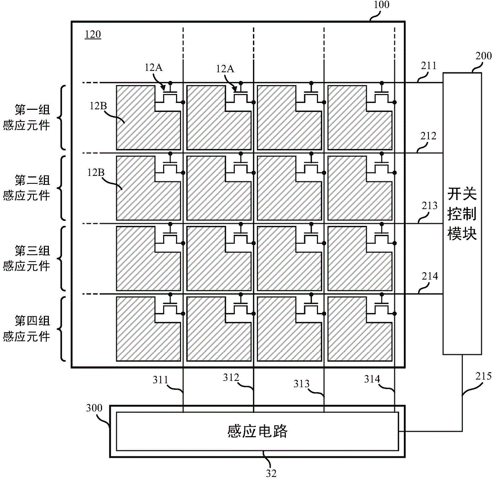
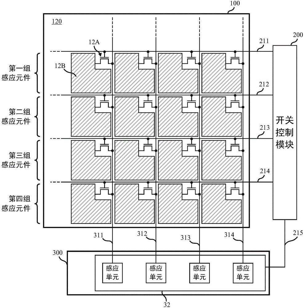
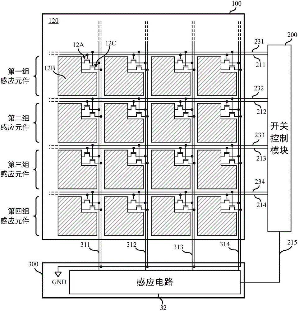
[0026] A specific embodiment according to the present invention is a sensing device, and its functional block diagram is shown in FIG. 1(A). The sensing device includes a substrate 100, a switch control module 200 and an integrated circuit 300. In practical applications, the sensing device can exist independently, or it can be integrated in various electronic products that need to sense the user's touch, such as mobile phones, notebook computers, and tablet computers. It should be noted that the sensing device according to the present invention can be used for fingerprint recognition, but the scope of the present invention is not limited to this.

[0027] A thin film transistor (TFT) structure 120 is formed on the substrate 100. The structure includes a plurality of thin film transistor switches 12A and a plurality of sensing electrodes 12B (shown as coated with diagonal stripes). In practice, the sensing electrode 12B can be realized by a metal layer or a metal alloy layer in ...


PUM


Abstract

The invention provides an induction device comprising a substrate, N groups of induction elements which are formed on the substrate, an induction circuit and a switch control module. Each group of induction elements include multiple induction elements. Each induction element includes a thin-film transistor switch and an induction electrode. The induction circuit is used for driving N groups of the induction elements so as to generate N groups of induction signals in order. The switch control module enables multiple induction elements included in one group of the induction elements of N groups of the induction elements to be connected to the induction circuit each time by controlling the thin-film transistor switches.

Description

technical field [0001] The present invention relates to a sensing device for detecting a user's touch. Background technique [0002] In order to improve data security, many electronic products have provided fingerprint identification functions in recent years. The most typical fingerprint identification device includes a sensing area with an area of ​​about one centimeter square, on which the user presses the front end of the finger. A plurality of sensing elements arranged in matrix form are arranged under the sensing area. Cooperating with the distance between two fingerprint protrusions of ordinary people, the number of sensing elements must be at least 100*100 (that is, about 10,000) to provide sufficient sensing resolution. If a self-capacitance sensing element is used, the fingerprint identification device is usually provided with the same number of sensing circuits as the sensing elements, respectively driving these sensing elements and receiving signals generated b...

Claims


Application Information

Patent Timeline
IPC IPC(8): G06K9/00
CPCG06V40/1318
Inventor 何闿廷
Owner MSTAR SEMICON INC
Why Eureka
Try Eureka