Semiconductor device, manufacturing method therefor, and electronic device
A manufacturing method and semiconductor technology, applied in semiconductor/solid-state device manufacturing, circuits, transistors, etc., can solve problems such as roll-up, affecting TiAl layer TiAl proportional load effect, etc., and achieve the effect of avoiding the upturning phenomenon
Active Publication Date: 2017-01-04
SEMICON MFG INT (SHANGHAI) CORP
View PDF7 Cites 0 Cited by
- Summary
- Abstract
- Description
- Claims
- Application Information
AI Technical Summary
Problems solved by technology
[0003] The existing technology usually adopts the atomic layer deposition process to form a TiAl layer as the work function metal layer of the NMOS. The deposition uses a Ti precursor and two Al precursors, and the two Al precursors are macromolecular substances. With the semiconductor With the continuous reduction of device fe
Method used
View moreImage
Smart ImageViewing Examples
Examples
 PUM
 Abstract
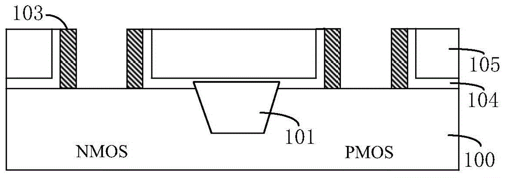
The invention provides a semiconductor device, a manufacturing method therefor, and an electronic device. The method comprises the steps: providing a semiconductor substrate with an NMOS region and a PMOS region, and forming a pseudo grid structure on the semiconductor substrate, wherein the pseudo grid structure comprises a sacrificial grid dielectric layer and a sacrificial grid electrode layer, and the sacrificial grid dielectric layer and the sacrificial grid electrode layer are overlapped from the bottom to the top; forming an interlayer dielectric layer on the semiconductor substrate, so as to achieve the filling of a gap between the pseudo grid structures; removing the pseudo grid structure, and forming a trench; forming a titanium-aluminium alloy layer, serving as a work function setting metal layer, in the trench through atomic layer deposition: carrying out the operations of aluminium precursor immersing and aluminium precursor stopping before the atomic layer deposition, wherein the operations of aluminium precursor immersing and aluminium precursor stopping are carried out sequentially for two times, and executing the aluminium precursor immersing operation of the same precursor as the injecting operation before the execution of the aluminium precursor injecting during the atomic layer deposition. According to the invention, the method can avoid the upwarp phenomenon of an NMOS work function.
Description
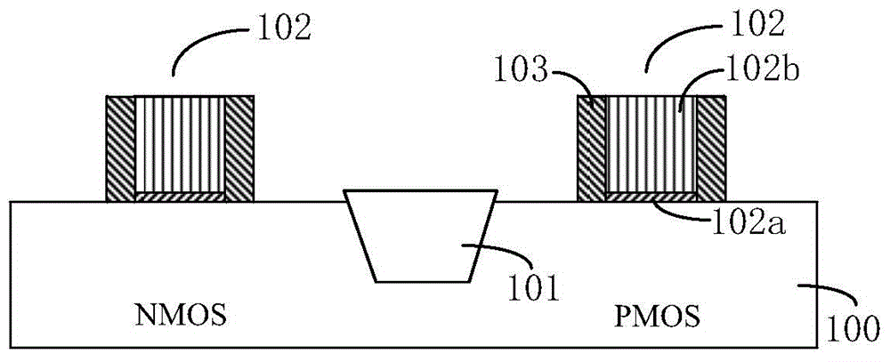
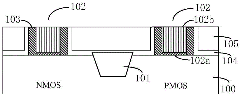
technical field [0001] The invention relates to a semiconductor manufacturing process, in particular to a semiconductor device, a manufacturing method thereof, and an electronic device. Background technique [0002] In the manufacturing process of next-generation integrated circuits, a high-k-metal gate process is usually used for the fabrication of complementary metal-oxide-semiconductor (CMOS) gates. For CMOS with a smaller numerical process node, the high-k-metal gate process is usually a gate-last process, and its implementation process is a high-k dielectric layer followed by a metal gate and a high-k dielectric layer followed by a There are two types of metal grids. The implementation process of the former includes: forming a dummy gate structure on a semiconductor substrate, and the dummy gate structure is composed of an interface layer, a high-k dielectric layer, a capping layer and a sacrificial gate material stacked from bottom to top. Layer composition; sidewall...
Claims
Login to View More Application Information
Patent Timeline
 IPC IPC(8): H01L21/8238H01L27/092
CPCH01L21/823828H01L27/092
Inventor 徐建华
Owner SEMICON MFG INT (SHANGHAI) CORP


