Film transistor and the manufacturing method thereof, array substrate and display apparatus

A technology of thin film transistors and substrate substrates, applied in the direction of transistors, semiconductor/solid-state device manufacturing, electric solid-state devices, etc., can solve the problems of reducing electron mobility, reducing on-state current, and large electron mobility

Active Publication Date: 2017-01-04
BOE TECH GRP CO LTD +1
View PDF3 Cites 15 Cited by
  • Summary
  • Abstract
  • Description
  • Claims
  • Application Information

AI Technical Summary

Problems solved by technology

However, in the prior art, the on-state current is increased by increasing the electron mobility between the source and the drain. In this way, when the TFT is in the off state, due to the electron mobility between the source and the drain Larger, making it difficult to form a complete PN structure on the drain side, which in tu

Method used


Image

  • Film transistor and the manufacturing method thereof, array substrate and display apparatus
  • Film transistor and the manufacturing method thereof, array substrate and display apparatus
  • Film transistor and the manufacturing method thereof, array substrate and display apparatus

Examples


Embodiment Construction

[0031] The following will clearly and completely describe the technical solutions in the embodiments of the present invention with reference to the accompanying drawings in the embodiments of the present invention. Obviously, the described embodiments are only some, not all, embodiments of the present invention. Based on the embodiments of the present invention, all other embodiments obtained by persons of ordinary skill in the art without making creative efforts belong to the protection scope of the present invention.

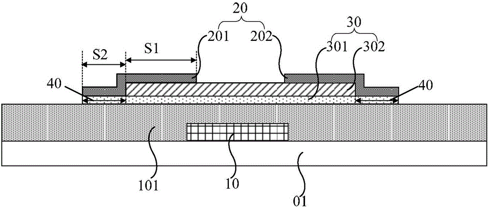
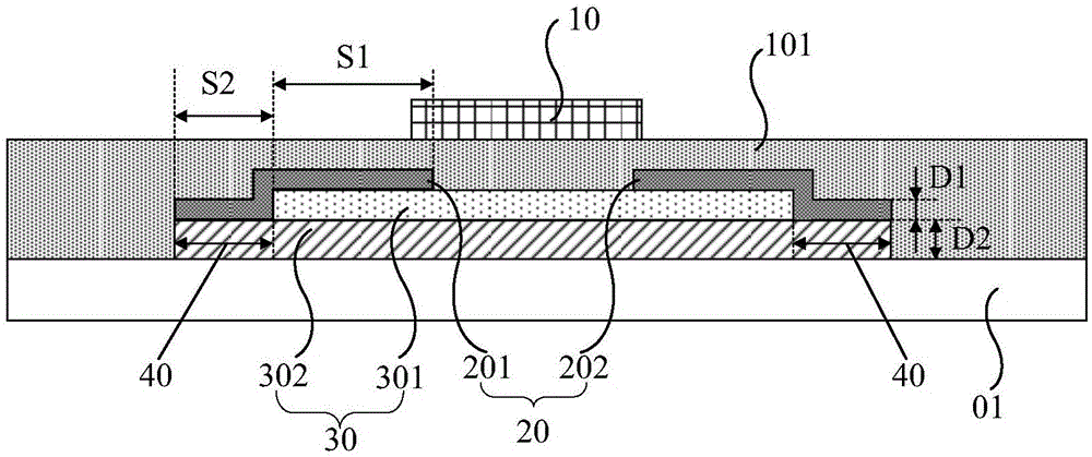
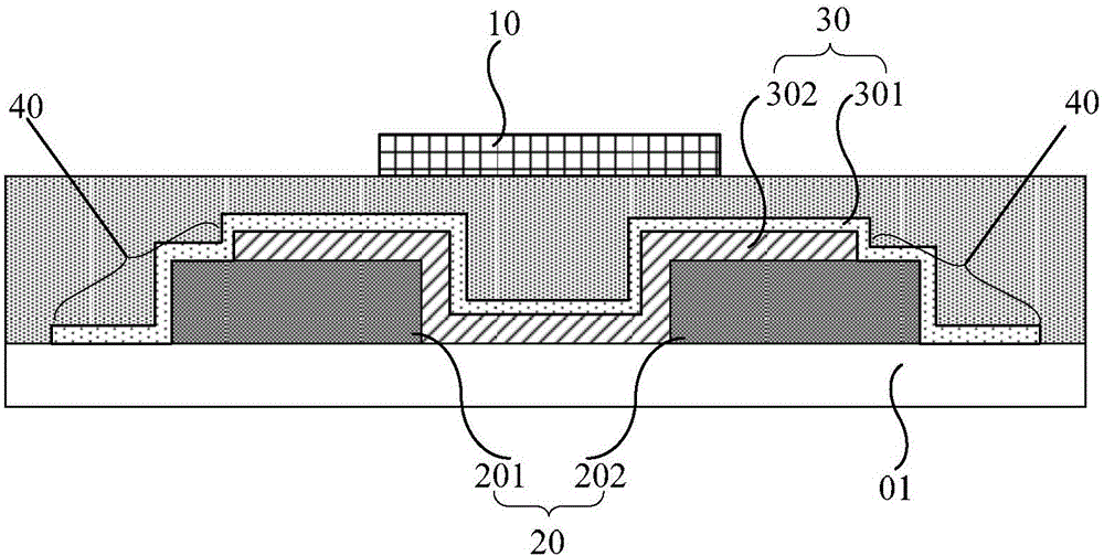
[0032] In this document, directional terms such as "upper", "lower", "left" and "right" are defined with respect to the directions in which the thin film transistors are schematically placed in the drawings, and it should be understood that these directional terms are relative Concepts, which are used for relative descriptions and clarifications, can change accordingly according to changes in the orientation in which the thin film transistors are placed.

[00...


PUM


Abstract

The embodiments of the present invention provide a film transistor and the manufacturing method thereof, an array substrate and a display apparatus, relating to the technical field of display and capable of effectively ensuring that while the on-state current is increased, the leakage current is reduced. The film transistor includes a gate electrode provided on a substrate, a source/drain pattern composed of a source electrode and a drain electrode, and an active layer, wherein the active layer comprises a first semiconductor layer and a second semiconductor layer arranged in layers, with the former having a larger electron mobility than the later and the former being closer to the gate electrode than the latter. The semiconductor layer at one side of the active layer and remote from the source/drain pattern has an extended part, compared with the semiconductor layer close to one side of the source/drain pattern, at a position corresponding to the source electrode and/or drain electrode. The source electrode and/or the drain electrode are in contact with the bottom surface of the semiconductor layer in the active layer close to one side of the source/drain pattern and extend to the extended part so that they are in contact with the extended part.

Description

technical field [0001] The invention relates to the field of display technology, in particular to a thin film transistor and a preparation method thereof, an array substrate, and a display device. Background technique [0002] With the continuous improvement of display technology, people's requirements for display devices are also constantly improving. Among various display technologies, TFT-LCD (Thin Film Transistor Liquid Crystal Display, thin film transistor liquid crystal display) technology because of its low energy consumption Advantages such as low cost and the like have been widely used in various display fields. [0003] Among them, two important indicators for evaluating the characteristics of TFT devices are on-state current and leakage current. The larger the on-state current and the smaller the leakage current, the better the performance of the TFT device. However, in the prior art, the on-state current is increased by increasing the electron mobility between t...

Claims


Application Information

Patent Timeline
IPC IPC(8): H01L29/786H01L27/12H01L21/336
CPCH01L27/1214H01L29/66742H01L29/786
Inventor 白金超刘建涛郭会斌
Owner BOE TECH GRP CO LTD
Why Eureka
Try Eureka