Relay circuit for half duplex communication and half duplex communication circuit
A relay circuit and half-duplex technology, applied in the field of half-duplex communication, to increase the number of nodes and reduce the distortion of data signals
- Summary
- Abstract
- Description
- Claims
- Application Information
AI Technical Summary
Problems solved by technology
Method used
Image

Examples
Embodiment 1
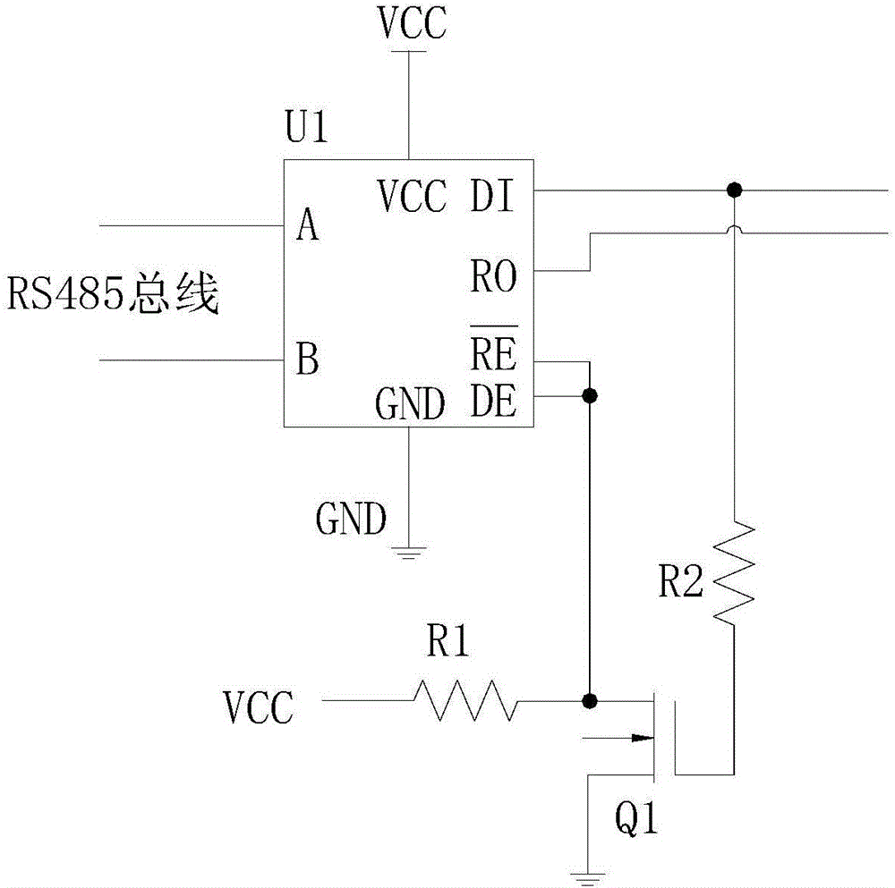
[0031] Reference figure 1 , Shows a transceiver circuit for half-duplex communication, which includes a communication chip U1, a switching device Q1, a resistor R1, and a resistor R2.
[0032] In the transceiver circuit, the communication chip U1 and the communication chip U2 are 485 chips, and the switching device Q1 and the switching device Q2 are field effect transistors. The communication chip can also be a chip for half-duplex communication such as the CC2520 zigbee chip. The switching device can also be a controllable switching device such as GTO, GTR or MOSFET.
[0033] In the transceiver circuit, the 485 chip U1 has two data transceiver terminals A and B, a receiving enable terminal DE, a transmission enable terminal RE, an output terminal RO, an input terminal DI, and a VCC terminal and A GND terminal; among them, the data transceiver terminals A and B are used to receive or send data signals; the receiving enable terminal DE is used to make the data transceiver terminal i...
Embodiment 2
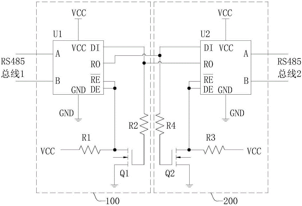
[0037] Reference figure 2 , Shows a relay circuit for half-duplex communication, which includes a 485 chip U1, a field effect transistor Q1, a resistor R1, a resistor R2, a 485 chip U2, a field effect transistor Q2, a resistor R3, and a resistor R4.
[0038] In the relay circuit, the 485 chip U1, the field effect transistor Q1, the resistor R1, and the resistor R2 constitute the above-mentioned transceiver circuit, which is hereinafter referred to as the first transceiver circuit 100; in the relay circuit, the 485 chip U2, the field The effect transistor Q2, the resistor R3, and the resistor R4 constitute another transceiver circuit described above, which is referred to as the second transceiver circuit 200 below.
[0039] In the first transceiver circuit 100 of the relay circuit, the 485 chip U1 has two data transceiver terminals A and B, a reception enable terminal DE, a transmission enable terminal RE, an output terminal RO, and an input terminal DI. And a VCC terminal and a GN...
Embodiment 3
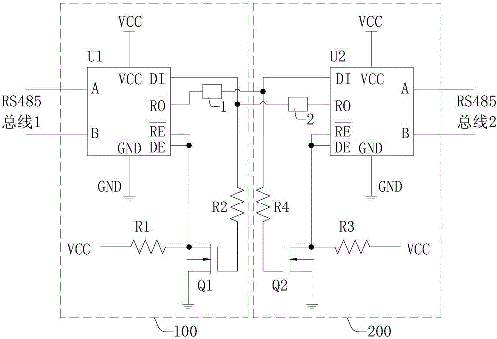
[0045] Reference image 3 , Shows a relay circuit for half-duplex communication, which is an improvement on the relay circuit provided in the second embodiment. Specifically, the output terminal of the first transceiver circuit 100 is coupled to the input terminal of the second transceiver circuit 200 through a signal holding unit 1, and the output terminal of the second transceiver circuit 200 is coupled to the first transceiver circuit 200 through a signal holding unit 1. The input terminal of the transceiver circuit 100.
[0046] In the relay circuit, the signal holding unit 1 may be a voltage follower, a signal holder, and other devices capable of maintaining a stable signal. In the relay circuit, the signal holding unit 1 can keep the digital signal output from the input terminal DI of the 485 chip U1 or the input terminal DI of the 485 chip U2 stable and improve the anti-interference performance.
PUM
 Abstract
Description
Claims
Application Information
 - R&D
- Intellectual Property
- Life Sciences
- Materials
- Tech Scout
- Unparalleled Data Quality
- Higher Quality Content
- 60% Fewer Hallucinations
Browse by: Latest US Patents, China's latest patents, Technical Efficacy Thesaurus, Application Domain, Technology Topic, Popular Technical Reports.
© 2025 PatSnap. All rights reserved.Legal|Privacy policy|Modern Slavery Act Transparency Statement|Sitemap|About US| Contact US: help@patsnap.com