Printed circuit board manufacturing method

A production method and circuit board technology, which is applied in multilayer circuit manufacturing, printed circuit manufacturing, printed circuit, etc., can solve problems such as difficult production, low yield rate, and easy breakage, so as to solve the problem of unstable connection and improve the use of Longevity, the effect of avoiding the fracture of the bending area and falling parts

Active Publication Date: 2017-01-04
惠州新联兴实业有限公司
View PDF5 Cites 1 Cited by
  • Summary
  • Abstract
  • Description
  • Claims
  • Application Information

AI Technical Summary

Problems solved by technology

However, there are many production processes of flexible and rigid boards, the production is difficult and the cycle is long, and the yield rate is low.
In the process of use, the bending part is prone to breakage, falling parts and other problems, which will affect the life of the entire electronic product

Method used


Image

  • Printed circuit board manufacturing method

Examples


Embodiment Construction

[0017] In order to facilitate the understanding of those skilled in the art, the present invention will be further described in detail below in conjunction with specific embodiments.

[0018] The circuit board manufacturing method of the present invention comprises the following seven steps:

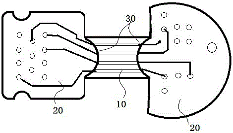
[0019] (1) Design the circuit graphics, drilling and shape data. In the circuit graphic design, only the connection circuit is designed in the part corresponding to the bending area, and the pads for welding devices are not set, that is, only the connection line is designed in the bending area and no electronic components are designed. Devices, arrange the electronic devices in the non-bending area of ​​the hard copper clad laminate and the copper clad soft laminate. And output image negatives according to the designed graphics. In addition, in the shape data design, the edge of the hard board corresponding to the junction of the non-bending area and the bending area needs to be designe...


PUM


Abstract

The invention provides a printed circuit board manufacturing method. The printed circuit board comprises a bent area and non-bent areas which are arranged at two sides of the bent area. The manufacturing method comprises the steps of (1), designing information of a circuit pattern, drilling holes and a profile, wherein only a connecting line is designed at a portion which corresponds with the bent area in designing the circuit pattern, and outputting an image negative film; (2), manufacturing a flexible copper-plated circuit board; (3), performing preprocessing on a hard copper-plated board and PP board; (4), pressing the flexible copper-plated board and the hard copper-plated board for combining; (5), drilling; (6), manufacturing a hard copper-plated circuit board; and (7), molding. According to the printed circuit board manufacturing method, a circuit board device and a line are reasonably planned, and furthermore an arc-shaped bent part is arranged at an area intersection, and problems such as fracture and component falling at the bent area can be effectively prevented, and service life of the circuit board is prolonged. According to the flexible bendable area in the circuit board, the flexible circuit board and the hard circuit board are pressed for forming a whole member, and a problem of unstable connection in a rigid-flexible printed circuit board in a buckle connecting form is effectively settled.

Description

technical field [0001] The invention relates to the technical field of printed circuit boards. Background technique [0002] At present, PCB board technology is developing in the direction of multi-layer and multi-functionalization. Many PCB boards need to be bent between different planes many times, which requires the substrate of PCB boards to have better flexibility. With the development and improvement of printed circuit technology, a rigid-flex PCB (Rigid-Flex PCB) has emerged. Rigid-flex boards have both the characteristics of FPC and PCB, and can be applied to some products with special requirements, such as military products. Rigid-flex boards play a great role in saving the internal space of products, reducing the volume of finished products, and improving product performance, so they are widely used. However, there are many production processes of soft and rigid boards, the production is difficult and the cycle is long, and the yield rate is low. During use, the...

Claims


Application Information

Patent Timeline
Patent Type & Authority Applications(China)
IPC IPC(8): H05K3/46H05K3/00
CPCH05K3/0044H05K3/4691H05K2201/2009H05K2203/061
Inventor 杨兴德
Owner 惠州新联兴实业有限公司
Why Eureka
Try Eureka