On-chip debug and diagnostic method, device and chip

An on-chip debugging and diagnosis method technology, applied in the field of integrated circuits, can solve the problems of the chip cannot automatically suspend fault diagnosis efficiency, low efficiency, etc., and achieve the effect of improving the debug ability, accurate fault location, and fast fault diagnosis.

Active Publication Date: 2017-01-11
LOONGSON TECH CORP
View PDF6 Cites 13 Cited by
  • Summary
  • Abstract
  • Description
  • Claims
  • Application Information

AI Technical Summary

Problems solved by technology

[0006] Embodiments of the present invention provide an on-chip debugging and diagnosis method, device, and chip to solve the problems that the chip cannot be automatically paused during debugging and the fault diagnosis efficiency is low

Method used


Image

  • On-chip debug and diagnostic method, device and chip
  • On-chip debug and diagnostic method, device and chip
  • On-chip debug and diagnostic method, device and chip

Examples


Embodiment Construction

[0026] In order to make the purpose, technical solutions and advantages of the embodiments of the present invention clearer, the technical solutions in the embodiments of the present invention will be clearly and completely described below in conjunction with the drawings in the embodiments of the present invention. Obviously, the described embodiments It is a part of embodiments of the present invention, but not all embodiments. Based on the embodiments of the present invention, all other embodiments obtained by persons of ordinary skill in the art without creative efforts fall within the protection scope of the present invention.

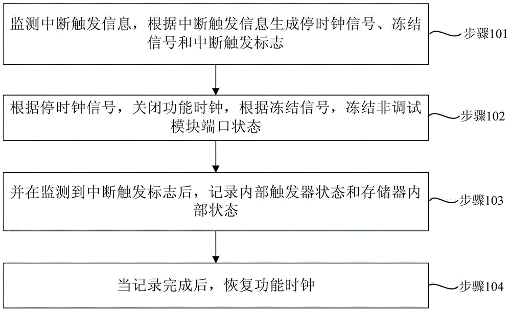
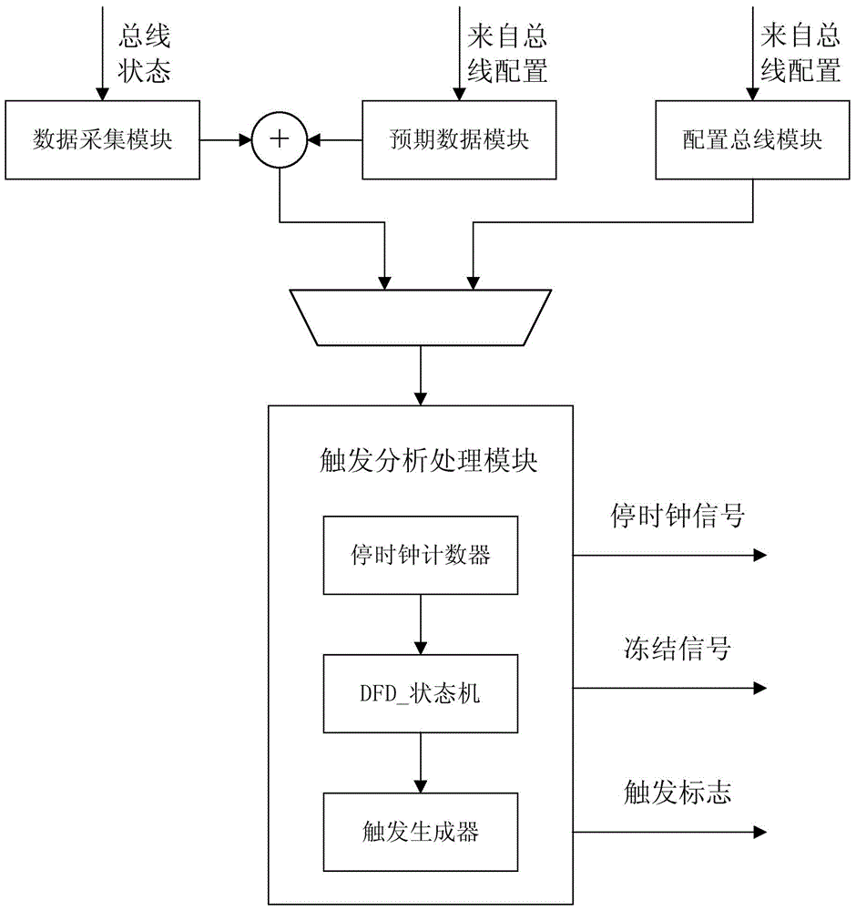
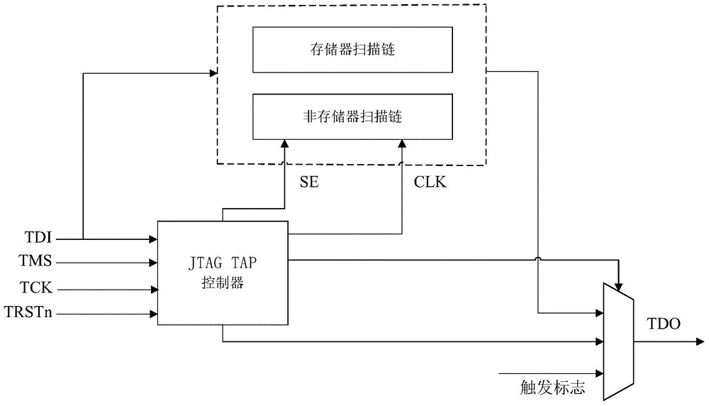
[0027] On the one hand, an embodiment of the present invention provides an on-chip debugging and diagnosis method, which is used for debugging and diagnosing a chip. The chip includes an on-chip debugging and diagnosis module and a chip main module, and the chip main module includes a debuggable module and a non-debuggable module. Such as figure...


PUM


Abstract

The present invention provides an on-chip debug and diagnostic method, a device and a chip. The method comprises the steps of monitoring the interrupt trigger information; generating a stop clock signal, a freeze signal and an interrupt trigger flag based on the interrupt trigger information; according to the stop clock signal, closing a functional clock; according to the freeze signal, freezing the state of a non-debug module port; upon monitoring the interrupt trigger flag, recording the state of an internal trigger and the internal state of a memory; after the recording is completed, recovering the function of the clock. Based on the on-chip debug and diagnostic method, the device and the chip, the functional clock can be automatically closed when the chip goes wrong, and the operation of a processor is paused. Meanwhile, the debug and diagnostic function is triggered automatically, so that the internal state of the chip can be quickly and accurately acquired. The debugging capability of the chip is effectively improved. therefore, the fault diagnosis is more rapid and the fault location is more accurate.

Description

technical field [0001] The invention relates to the field of integrated circuits, in particular to an on-chip debugging and diagnosis method, device and chip. Background technique [0002] With the increasing design scale of chips in the current integrated circuit field, the complexity and integration are getting higher and higher, but the timeliness of chips from design to market is also becoming more and more stringent. These factors make the silicon front of the chip Validation is difficult to do adequately. Due to insufficient pre-silicon verification of the chip, it may lead to failure of the chip after tape-out. For these failures, debugging and diagnosis are usually carried out by means of post-silicon debugging. [0003] The traditional post-silicon debugging method is slightly different due to different chips. Usually, the chip is in a functional mode (that is, running a normal function), and the method of recording and analyzing the input and output of the chip i...

Claims


Application Information

Patent Timeline
Patent Type & Authority Applications(China)
IPC IPC(8): G01R31/28
Inventor 陈华军娄卓阳刘慧王焕东齐子初王琳
Owner LOONGSON TECH CORP
Why Eureka
Try Eureka