Display substrate as well as driving method and preparation method thereof, display panel and display device

A technology of display substrate and driving method, applied in nonlinear optics, instruments, optics, etc., can solve problems such as inability to adjust on-current and increased power consumption.

Inactive Publication Date: 2017-01-11
BOE TECH GRP CO LTD +1
View PDF6 Cites 0 Cited by
  • Summary
  • Abstract
  • Description
  • Claims
  • Application Information

AI Technical Summary

Problems solved by technology

[0003] However, there are at least the following problems in the prior art: to control the current through different channel width-to-length ratios, in fact, in the process of preparing TFT, a fixed mask needs to be used, so the width-to-length ratio of the channel of the TFT is practical is fixed, so the conduction current I on and closing current I off It is also fixed, and it is impossible to adjust the conduction current I on and closing current I off The purpose; while controlling the current through the driving voltage, because the current corresponding to different driving voltages is fixed (such as figure 1 shown), if you want to increase the current, you must increase the driving voltage, but the increase in the driving voltage will lead to increased power consumption

Method used


Image

  • Display substrate as well as driving method and preparation method thereof, display panel and display device
  • Display substrate as well as driving method and preparation method thereof, display panel and display device
  • Display substrate as well as driving method and preparation method thereof, display panel and display device

Examples


Embodiment 1

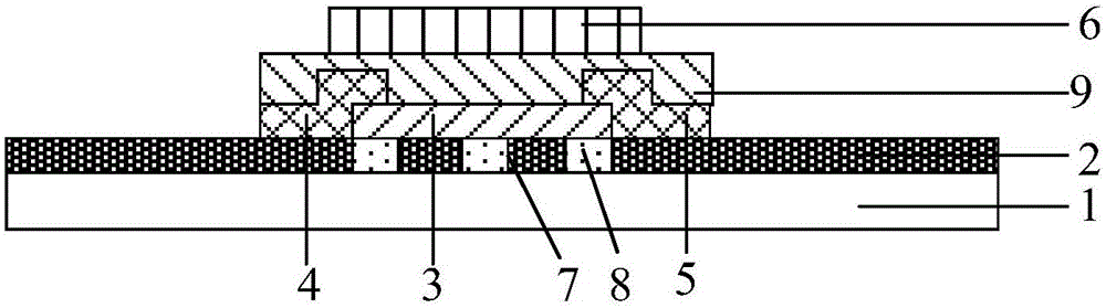
[0040] Please refer to Figure 2 to Figure 4 This embodiment provides a display substrate, including a base substrate 1, a black matrix layer 2, and a thin film transistor; the thin film transistor includes an active layer 3, a source electrode 4, a drain electrode 5, and a gate electrode 6; the black matrix layer 2 is located on the substrate On the base substrate 1, the active layer 3, the source 4 and the drain 5 are all located above the black matrix layer 2, the source 4 and the drain 5 are respectively connected to the active layer 3, and the gate 6 is located on the active layer 3. Above.

[0041] Such as figure 2 As shown, the display substrate further includes a gate insulating layer 9. Among them, the black matrix layer 2 is located on the base substrate 1, the active layer 3 is located on the black matrix layer 2, part of the source electrode 4 is located on the active layer 3, part of the drain electrode 5 is located on the active layer 3, and the gate insulating lay...

Embodiment 2

[0056] Please refer to Figure 5 This embodiment provides a method for driving a display substrate. The display substrate is the display substrate of Embodiment 1. The driving method includes:

[0057] Step S1, applying a first level to the gate to turn on the thin film transistor and make the electrochromic material in a light-transmitting state.

[0058] Step S2, applying a second level to the gate to turn off the thin film transistor and make the electrochromic material in a dark state.

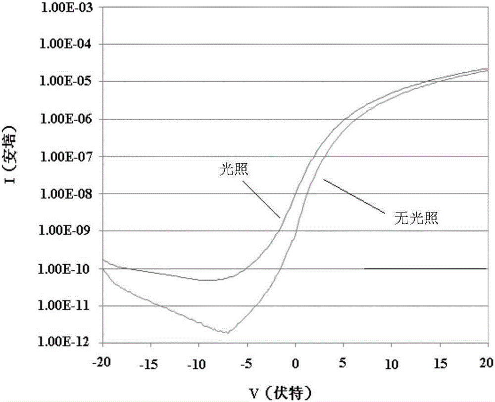
[0059] It should be noted that after applying the first level or the second level to the gate, the gate will form a vertical downward electric field, that is, the direction of the electric field points to the electrochromic material, and the vertical downward electric field changes the electrochromic material The state (transparent state or dark state). Of course, the grid can also be combined with other electrodes to form an electric field, as long as the state of the electrochromic material ca...

Embodiment 3

[0066] Please refer to Figure 6 to Figure 11 , This embodiment provides a method for manufacturing a display substrate, including:

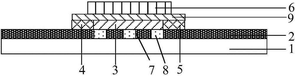
[0067] Step 101, forming a black matrix layer 2 on the base substrate 1, such as Figure 7 Shown.

[0068] Step 102, forming a hollow pattern 7 in the black matrix layer 2, such as Figure 8 Shown.

[0069] Step 103, arrange electrochromic material 8 in the hollow pattern 7, such as Picture 9 Shown.

[0070] Step 104, forming an active layer 3, a source electrode 4 and a drain electrode 5 on the black matrix layer 2. The source electrode 4 and the drain electrode 5 are respectively connected to the active layer 3, and the hollow pattern 7 corresponds to at least part of the active layer 3 Settings such as Picture 10 Shown.

[0071] Of course, after step 104, it also includes:

[0072] Step 105, forming a gate insulating layer 9 on the active layer 3, the source electrode 4 and the drain electrode 5, such as Picture 11 Shown.

[0073] Step 106, forming ...


PUM


Abstract

The invention provides a display substrate as well as a driving method and a preparation method thereof, a display panel and a display device, belongs to the technical field of display and can solve the problem of power consumption increase cause by the fact that breakover current Ion of a TFT (thin-film transistor) is increased by increasing driving voltage at present. The display substrate comprises a substrate body, a black matrix layer and a TFT, wherein the TFT comprises an active layer, a source, a drain and a gate; the black matrix layer is located on the substrate body, the active layer, the source and the drain are all located above the black matrix layer, the source and the drain are connected with the active layer respectively, and the gate is located above the active layer; the black matrix layer comprises hollowed-out patterns which are arranged corresponding to at least part of the active layer, and electrochromic materials are arranged in the hollowed-out patterns.

Description

Technical field [0001] The present invention belongs to the field of display technology, and specifically relates to a display substrate, a driving method and preparation method thereof, a display panel, and a display device. Background technique [0002] In the existing display technology, a thin-film transistor (TFT for short) is a core component in a display device. The ideal TFT needs to meet the following conditions, that is, the conduction current I when it is turned on on Maximum, and closed current I when closed off As small as possible. To achieve this goal, existing TFT designs can only adjust its performance through different channel width-to-length ratios or driving voltages. [0003] However, there is at least the following problem in the prior art: the current is controlled by different channel width-to-length ratios. In fact, in the process of preparing TFTs, a fixed mask is required. Therefore, the width-to-length ratio of the TFT channels is actually Is fixed, s...

Claims


Application Information

Patent Timeline
Patent Type & Authority Applications(China)
IPC IPC(8): G02F1/1335G02F1/1333
CPCG02F1/1333G02F1/133512
Inventor 董殿正王俊伟张斌张强解宇王光兴张衎陈鹏名
Owner BOE TECH GRP CO LTD
Why Eureka
Try Eureka