System and method for detecting defects of blind holes in PCB (Printed Circuit Board) bare board based on AOI (Automated Optical Inspection)

A detection system and detection method technology, applied in image data processing, instruments, calculations, etc., can solve the problem of low blind hole detection accuracy, and achieve the effects of reducing noise interference, reducing system cost, and improving accuracy

Active Publication Date: 2017-01-11
XIDIAN UNIV
View PDF7 Cites 13 Cited by
  • Summary
  • Abstract
  • Description
  • Claims
  • Application Information

AI Technical Summary

Problems solved by technology

[0006] The purpose of the present invention is to overcome the above-mentioned defects in the prior art. The present invention proposes an AOI-based PCB blind hole defect detection s

Method used


Image

  • System and method for detecting defects of blind holes in PCB (Printed Circuit Board) bare board based on AOI (Automated Optical Inspection)
  • System and method for detecting defects of blind holes in PCB (Printed Circuit Board) bare board based on AOI (Automated Optical Inspection)

Examples


Embodiment Construction

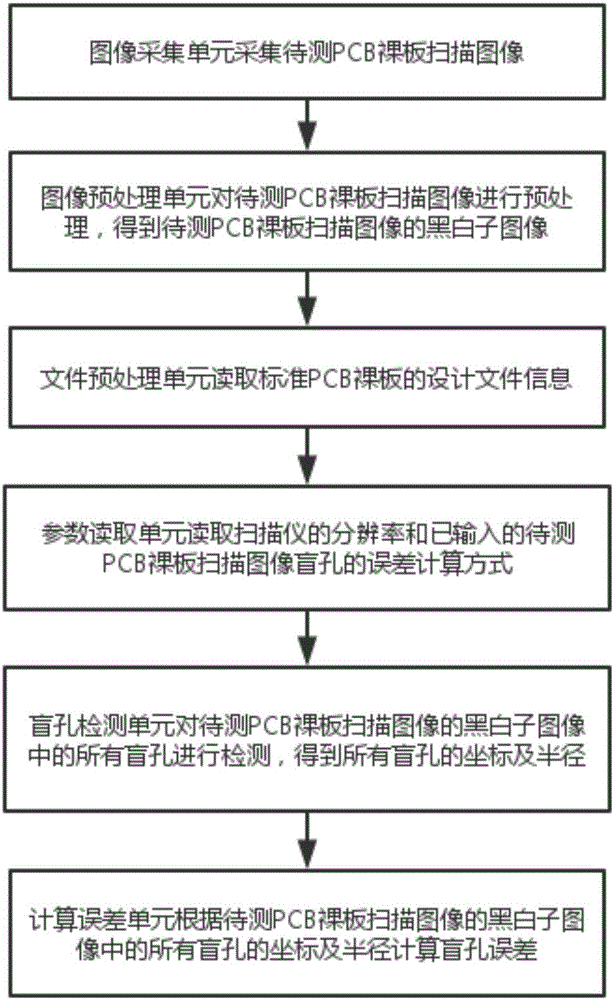
[0038] The present invention will be described in further detail below in conjunction with the accompanying drawings and embodiments.

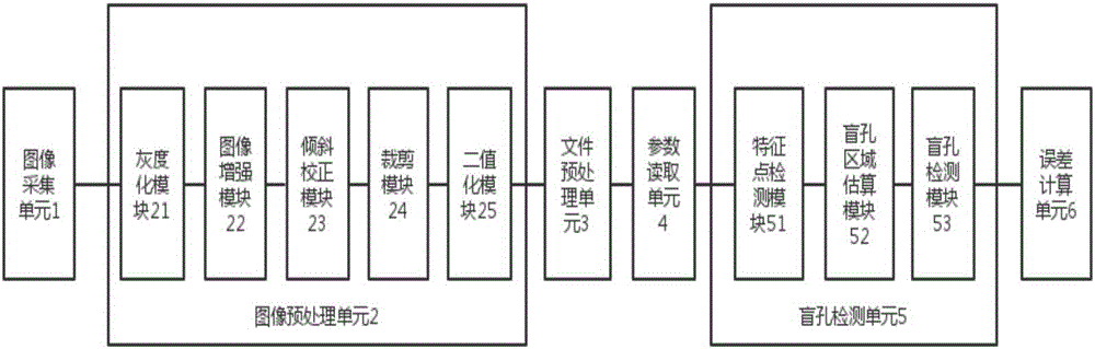
[0039] refer tofigure 1 , the detection system of the present invention includes an image acquisition unit, an image preprocessing unit, a file preprocessing unit, a parameter reading unit, a blind hole detection unit and an error calculation unit connected in sequence, wherein:

[0040] An image acquisition unit, configured to acquire a scanned image of a bare PCB to be tested;

[0041] An image preprocessing unit is used to preprocess the scanned image of the PCB bare board to be tested;

[0042] The file preprocessing unit is used to read the coordinate value representation form, mounting hole information and blind hole information in the standard PCB bare board design file;

[0043] The parameter reading unit is used to read the resolution of the scanner and the error calculation method of the blind hole of the scanned image of the PCB ba...


PUM


Abstract

The invention provides a system and a method for detecting defects of blind holes in a PCB (Printed Circuit Board) bare board based on AOI (Automated Optical Inspection). The system and the method are used for solving the technical problem of low detection accuracy of blind holes in dark in the existing detection system and method. The detection system comprises an image acquisition unit, an image preprocessing unit, a file preprocessing unit, a parameter reading unit, a blind hole detection unit and an error calculation unit; and the method comprises the steps of firstly, acquiring a scan image of a PCB bare board to be detected, preprocessing the scan image to obtain a binary image, then reading design file information of a standard PCB bare board, detecting coordinates and radii of all blind holes in the binary image according to the design file information of the standard PCB bare board, and finally calculating errors of all blind holes on the scan image of the PCB bare board to be detected. The detection accuracy in dark is high, the cost of the system is low, and the system and the method can be used for detecting defects of blind holes in circuit board machining environments.

Description

technical field [0001] The invention belongs to the technical field of circuit board detection, relates to graphic image processing technology, and in particular to an AOI-based detection system and method for blind hole defects of PCB bare boards, which can be used for detection of blind hole defects in circuit board processing environments. Background technique [0002] A printed circuit board (PCB, Printed Circuit Board) is a provider of electrical connections for electronic components. It is the foundation of the modern information industry. Small and medium-sized equipment ranging from electronic watches, electric toys to TVs, smart household appliances, and then to electronic communication equipment, military weapon systems, space shuttles and other large equipment cannot do without it. It plays an important role in life, It plays a major role in society, transportation, aerospace and other aspects. With the development of electronics industry and surface mount techno...

Claims


Application Information

Patent Timeline
IPC IPC(8): G06T7/00G06T5/00
CPCG06T5/001G06T7/0008G06T2207/10004G06T2207/30141
Inventor 臧明相刘静来新泉袁冰王振轩陈斌
Owner XIDIAN UNIV
Why Eureka
Try Eureka