All-period-luminosity LED lamp with LED inverted wafer

A technology of LED lamps and chips, which is applied in the direction of electrical components, electric solid devices, circuits, etc., can solve the problems of inconvenient production and equipment, unreasonable LED chip circuit layout, and unreasonable circuit layout, etc., to achieve uniform luminosity Effect

Inactive Publication Date: 2017-01-25
莆田莆阳照明有限公司 +1
View PDF11 Cites 4 Cited by
  • Summary
  • Abstract
  • Description
  • Claims
  • Application Information

AI Technical Summary

Problems solved by technology

[0002] LED light tube is also called fluorescent tube. Its light source adopts LED as illuminant. LED is a solid-state semiconductor light-emitting device. As a new generation of light source, it is developing rapidly. It can directly convert electricity into light, and has low-voltage power supply. Low electricity, strong applicability and high stability; LED chips are the main raw materials of LEDs, and LEDs mainly rely on chips to emit light. There are problems of long packaging process cycle time and low success rate, inconvenient production and equipment, which increase the production cost of LED lamps;
[0003] Patent No. CN204189826U patent document, patent No. CN204315628U patent document and patent No. CN204315621U patent document disclose LED light source flip-chip technology; The problem of low success rate; however, the current LED light source flip-chip technology is mainly used on metal substrates such as aluminum and copper or on ceramic substrates. Due to the influence of the light transmittance of the substrate, the light angle of the light source module is also limited, so it cannot be done. The light spot is consistent up to 360 degrees; and because the LED flip chip itself only emits light from five sides, the side with electrodes is affected by the electrode and insulating layer and the light effect cannot be emitted, which also makes the chip substrate unable to achieve a 360-degree full-circle light spot unanimous

Method used


Image

  • All-period-luminosity LED lamp with LED inverted wafer

Examples


Embodiment Construction

[0027] The technical solutions of the present invention will be further described in detail below in conjunction with specific embodiments.

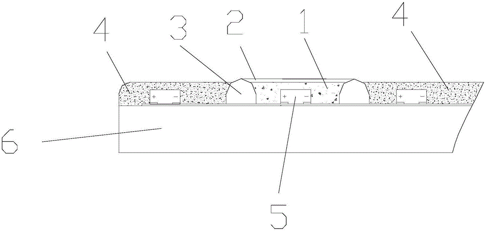
[0028] see figure 1 , a full-circumference LED lamp with LED flip-chip, comprising a light source, the light source includes a substrate 6, an LED flip-chip 5, a reflective structure 2 and a fluorescent adhesive layer; the light source includes a substrate 6, and the substrate 6 The upper surface is provided with a circuit layer, the circuit layer is provided with an electrical connection point of the LED chip, and the LED flip chip 5 is installed on the upper side of the substrate 6, and the LED flip chip 5 and the LED chip on the substrate 6 are electrically connected. The connection point is connected; the surrounding surface of the LED flip chip 5 is coated with a fluorescent adhesive layer, and a reflective structure 2 is also arranged on the fluorescent adhesive layer directly above the LED chip 5, and the area of ​​the reflective ...


PUM


Abstract

The invention discloses an all-period-luminosity LED lamp with an LED inverted wafer. The all-period-luminosity LED lamp comprises a light source, wherein the light source comprises a substrate and the LED inverted wafer, and the LED inverted wafer is mounted on the upper side of the substrate; the substrate is a transparent substrate, and the circumferential surface of the LED inverted wafer is coated with a fluorescent glue layer; a light reflecting structure is arranged on the surface of the fluorescent glue layer on an LED wafer, and the area of the light reflecting structure is 1 / 2 of that of the fluorescent glue layer; and a circuit layer is arranged on the upper surface of the substrate, an electric connecting point of the LED wafer is arranged on the circuit layer, and the LED inverted wafer is connected with the electric connecting point of the LED wafer on the substrate. According to the all-period-luminosity LED lamp, a dark region is compensated by a lighting part through reflected light of the light reflecting structure, and finally the luminosity of the whole lamp is uniform.

Description

technical field [0001] The invention relates to the field of LED lighting lamps, in particular to a full-circumference LED lamp with an LED flip-chip chip. Background technique [0002] LED light tube is also called fluorescent tube. Its light source adopts LED as illuminant. LED is a solid-state semiconductor light-emitting device. As a new generation of light source, it is developing rapidly. It can directly convert electricity into light, and has low-voltage power supply. Low electricity, strong applicability and high stability; LED chips are the main raw materials of LEDs, and LEDs mainly rely on chips to emit light. There are problems of long packaging process cycle time and low success rate, inconvenient production and equipment, which increase the production cost of LED lamps; [0003] Patent No. CN204189826U patent document, patent No. CN204315628U patent document and patent No. CN204315621U patent document disclose LED light source flip-chip technology; The proble...

Claims


Application Information

Patent Timeline
Patent Type & Authority Applications(China)
IPC IPC(8): H01L33/60H01L25/075
CPCH01L33/60H01L25/0753
Inventor 陈春松罗二强李国华林建先
Owner 莆田莆阳照明有限公司
Why Eureka
Try Eureka