
Display device and production method for pixel forming structure of organic electronic assembly

A technology of organic electronics and a manufacturing method, which is applied in the field of manufacturing the pixel formation structure of displays and organic electronic components, and can solve the problems of shrinking pixel display area 13, uneven light emission of the display, insufficient light emission brightness of the display, etc.

Inactive Publication Date: 2007-06-27
DELTA OPTOELECTRONICS
View PDF0 Cites 0 Cited by
  • Summary
  • Abstract
  • Description
  • Claims
  • Application Information

AI Technical Summary

Problems solved by technology

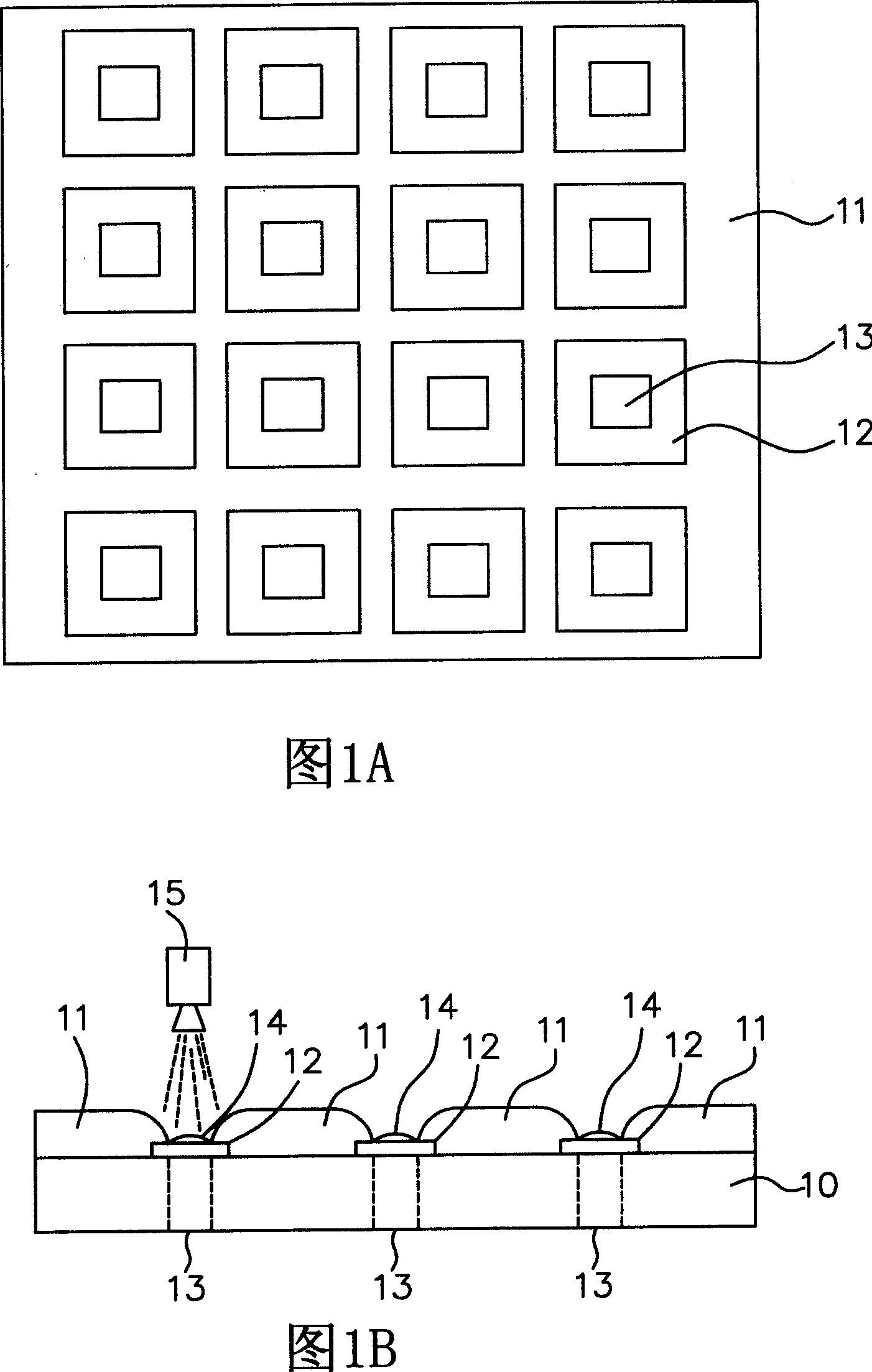
[0003] The first is to make the pixel display area 13 shrink accordingly, causing the problem of insufficient brightness of the display
[0004] The second is that the four perimeters of the effective pixels are all made of protruding insulating materials. When the ink is sprayed on the effective pixels, it will cause the liquid ink 14 to form a surface tension phenomenon. The central area is thicker and the surroundings are thinner, causing the display to glow. Inhomogeneity

Method used


Image

  • Display device and production method for pixel forming structure of organic electronic assembly
  • Display device and production method for pixel forming structure of organic electronic assembly
  • Display device and production method for pixel forming structure of organic electronic assembly

Examples


Embodiment Construction

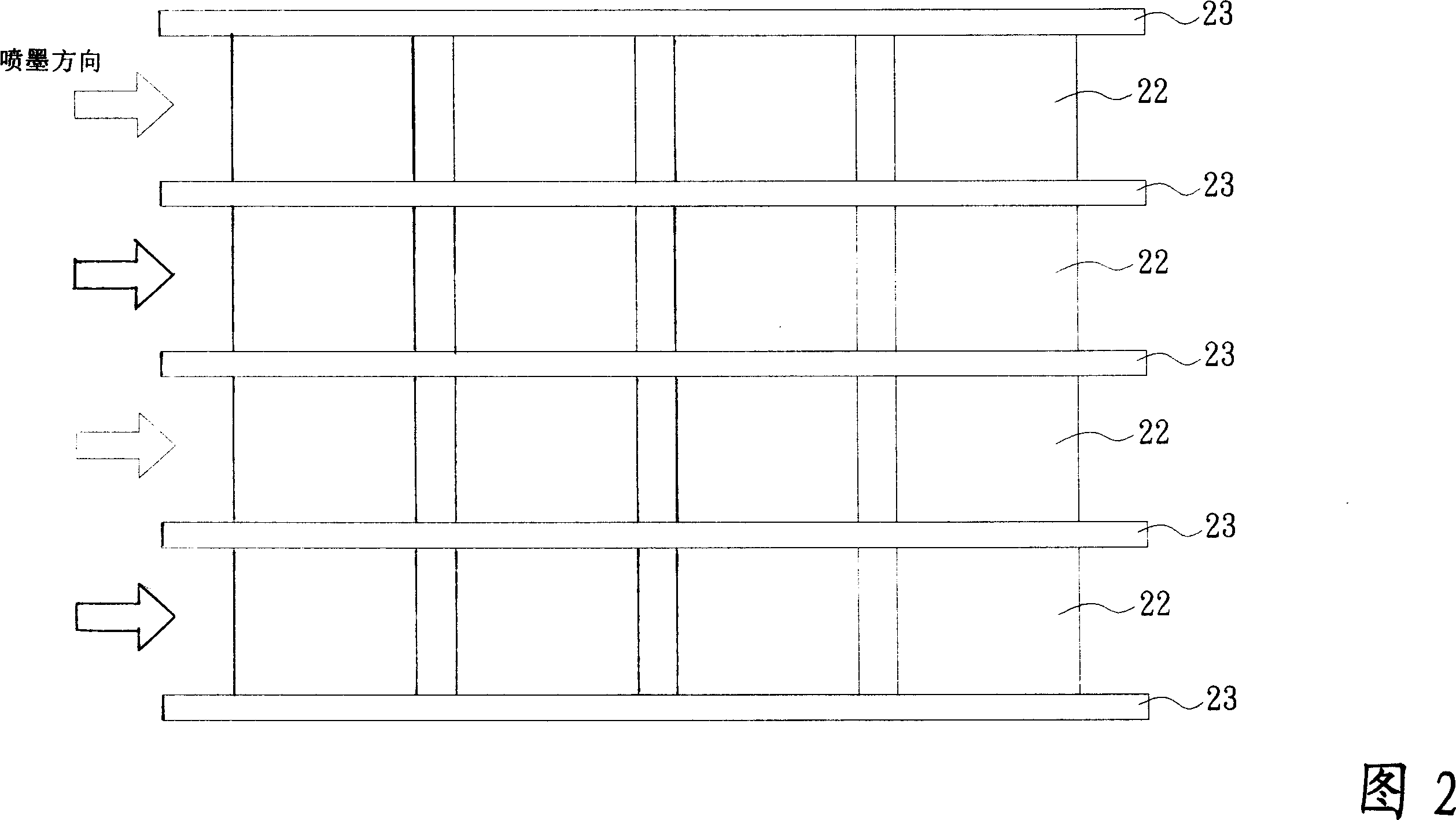
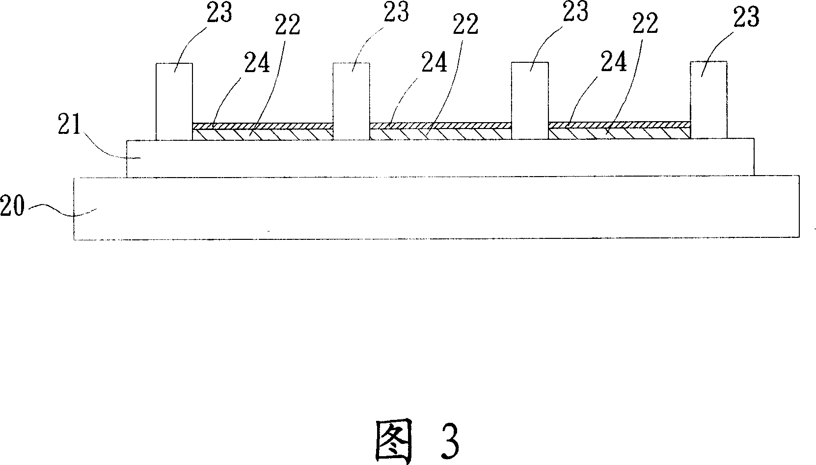
[0021] Please refer to Fig. 1 and Fig. 3, which are schematic diagrams of the pixel formation structure of the display of the present invention, wherein the light source of the display is composed of a polymer light-emitting diode (Polymer OLED, PLED), and the display has the characteristics of active light emission. It is very suitable as a light-emitting display panel for a display, and has the advantages of power saving and good brightness. At the same time, the manufacturing process of the present invention is not limited to the manufacturing process of the display, and also includes, for example, the manufacturing process of organic electronic components (Organic Electronic). Applicable technical means of the present invention, this technical means is to use insulating material (Bank) 23 to arrange liquid ink with single vertical or horizontal direction on the two peripheries parallel to picture element (Pixel) 22 in the manufacturing process, and this insulating material 2...


PUM


Abstract

The invention is a display and a facture method of a picture-pixel forming sturcture of an organic electronic assembly, in which liquid ink is provided in a single longitudinal direction or a transverse direction to form two edges which are in parallel in the picture-pixels by using an insulating material, arranging direction of the insulating material is vertical to an arranging direction of an anode formed on coating indium tin-doped oxide (ITO) of a transparent glass substrate but not surround around four edges of the picture-pixel. When performing an ink jetting program, a row or a column is acted as an operation unit but not using a single picture-pixel as an ink jetting unit, so that each picture-pixel is formed evenly, and irradiance of the display is even. On the other hand, the arranging direction of the insulating material is in parallel with a cathode forming direction, the picture-pixels is jetted and formed at surfaces of the anodes by an int jetting device, the insulating material is two cathode separating strips adjacent with each other to ensure accuracy of the display picture-pixel facture process and increase irradiance area and uniformity of each picture-pixel.

Description

technical field [0001] The present invention relates to a manufacturing method of a pixel forming structure of a display and an organic electronic component, especially a method of using an insulating material to arrange a liquid ink on two parallel peripheries of a pixel in a single vertical or horizontal direction during the manufacturing process, and to insulate The arrangement direction of the material is perpendicular to the arrangement direction of the anode formed by coating Indium Tin-doped Oxide (ITO) on the transparent glass substrate, instead of enclosing the surrounding of the pixel, it can be done or It is listed as an operation unit instead of the existing single pixel as the inkjet unit, so the formation of each pixel is very flat and uniform, so the luminosity of the display can be made uniform, and on the other hand, the arrangement direction of the insulating material is exactly the same as that of the cathode The formation direction is parallel, and the pixe...

Claims


Application Information

Patent Timeline
IPC IPC(8): H05B33/10H05B33/12
Inventor 林立基李玉山森育雄廖麒贵陈纯鉴
Owner DELTA OPTOELECTRONICS
Learn More