Flexible printed circuit board, display and flexible printed circuit board manufacturing method
A flexible printed circuit, flexible printing technology, applied in the direction of printed circuit, printed circuit, printed circuit parts, etc., can solve the problem of FPC impedance not too high, and achieve the effect of not too high impedance
- Summary
- Abstract
- Description
- Claims
- Application Information
AI Technical Summary
Problems solved by technology
Method used
Image
Examples
Embodiment 1
[0054] In order to solve the problem in the prior art of how to keep the impedance of the FPC from being too high while ensuring that the size of the FPC is not too large, an embodiment of the present application provides an FPC.
[0055]The FPC includes several pins, and the several pins are arranged on the FPC. The main feature of the FPC provided in the embodiment of the present application is that it is arranged on the above-mentioned several pins on the flexible printed board, has the same function and is adjacent to each other. There is no space between the arranged pins, that is, the space is 0.
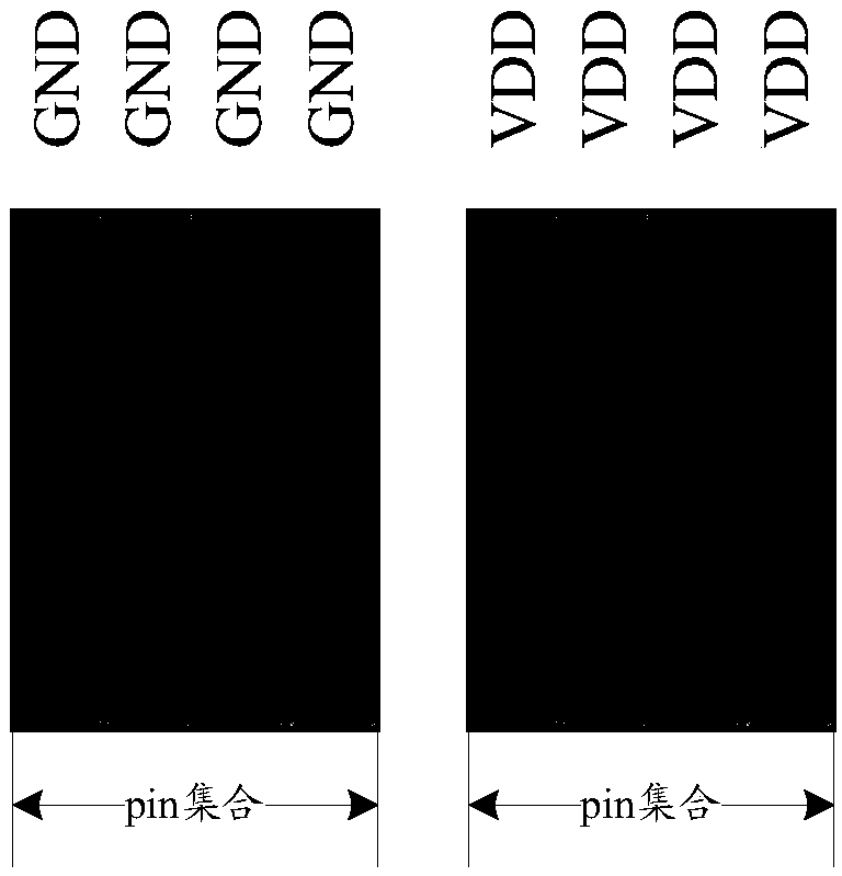
[0056] In the embodiment of the present application, all pins that have the same function and are adjacently arranged can be regarded as forming a set of pins. for example, figure 2 Each of the pins named "GND" in , because their functions are grounding, so they are pins with the same function; each pin named "VDD", because their functions are connected to the power supply, ...
Embodiment 2
[0063] Embodiment 2 provides an FPC that can be used for bonding with a display screen. Such as Figure 6 Shown is a schematic structural diagram of the FPC provided in Example 2.
[0064] Such as Figure 6 As shown, the FPC includes pins respectively: GND pin, VDD pin, VCI pin, D1, D2, and D3-Dn.
[0065] In order to maintain the clarity of the drawing, pins such as D3~Dn are omitted in the figure. In addition, the symbol "+" in the figure represents an alignment mark (mark), and the symbol "+" in other figures is also used to represent an alignment mark, which will not be repeated here.
[0066] exist Figure 6 In the FPC shown, there is no gap between the four adjacently arranged GND pins, that is, the distance between the four adjacently arranged GND pins is 0; similarly, between the four VDDs, There is also no gap, that is, the distance between 4 adjacently arranged VDD pins is 0. However, for pins that are adjacently arranged but have different functions, such as D...
Embodiment 3
[0071] Generally, in practical applications, the impedance of the VDD pin and the GND pin is required to be low—for example, the impedance of the VDD pin and the GND pin is generally required to be no more than 2 ohms; for some signal pins, it is not required Its impedance is low - for example, the impedance of a single signal pin is within 100 ohms, which can be considered as meeting the requirements. Therefore, if according to figure 2 or as Figure 7 In the prior art shown, setting the vertical height of the signal pin to be the same as that of the VDD pin and the GND pin so as to reduce the impedance of the signal pin is actually not necessary.
[0072] Based on the above analysis, Embodiment 3 provides an FPC. Such as Figure 8 Shown is a schematic structural diagram of the FPC provided in Example 3.
[0073] Such as Figure 8 As shown, the FPC includes pins respectively: GND pin, VDD pin, VCI pin, D1, D2, and D3-Dn.
[0074] with such figure 2 Compared with the ...
PUM
 Abstract
Description
Claims
Application Information


