Display substrate and manufacturing method thereof and display device and maintenance method thereof

A display substrate and display unit technology, applied in nonlinear optics, instruments, optics, etc., can solve the problem of low welding success rate and achieve the effect of improving the welding success rate

Pending Publication Date: 2017-02-15
HEFEI XINSHENG OPTOELECTRONICS TECH CO LTD +1
View PDF5 Cites 8 Cited by
  • Summary
  • Abstract
  • Description
  • Claims
  • Application Information

AI Technical Summary

Problems solved by technology

[0006] The present invention provides a display substrate and its manufacturing method, a display device and its maintenance method, which are used to solve the problem of low welding success rate when grid line signals are introduced into pixel electrodes by welding

Method used


Image

  • Display substrate and manufacturing method thereof and display device and maintenance method thereof
  • Display substrate and manufacturing method thereof and display device and maintenance method thereof
  • Display substrate and manufacturing method thereof and display device and maintenance method thereof

Examples


Embodiment Construction

[0042] The specific implementation manner of the present invention will be further described in detail below with reference to the drawings and embodiments. The following examples are used to illustrate the present invention, but are not intended to limit the scope of the present invention.

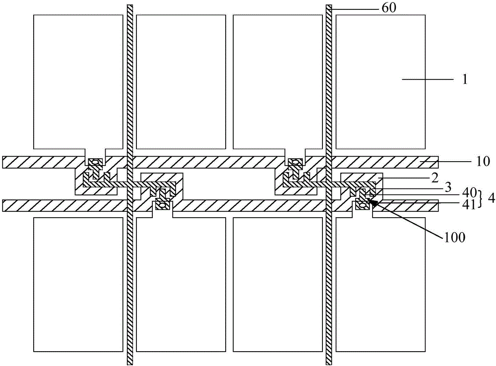
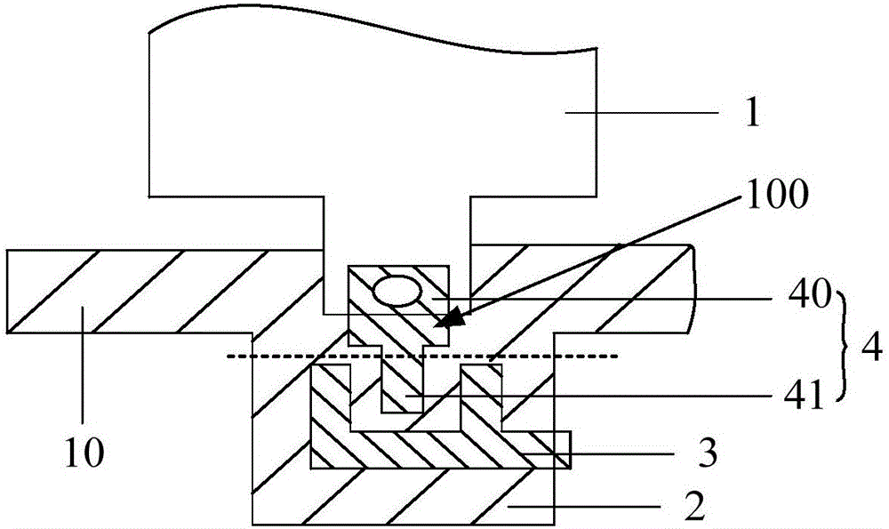
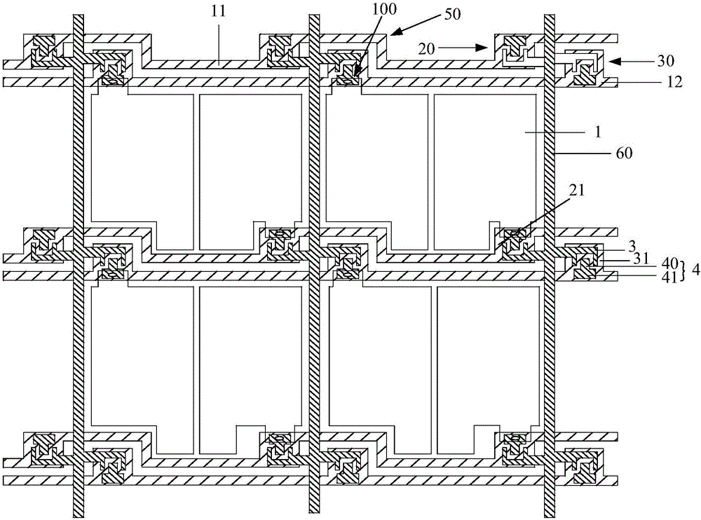
[0043] combine figure 1 and image 3 As shown, an embodiment of the present invention provides a display substrate, including:

[0044] A plurality of gate lines 10 and a plurality of data lines 60, the gate lines 10 and the data lines 60 intersect to define a plurality of pixel areas;

[0045] A plurality of display units, each display unit comprising:

[0046] a pixel electrode 1 arranged in the pixel area;

[0047] A thin film transistor for transmitting voltage to the pixel electrode 1, the gate electrode 2 of the thin film transistor is electrically connected to the gate line 10, the source electrode 3 is electrically connected to the data line 60, and the drain electrode 4 is el...


PUM


Abstract

The invention relates to the technical field of display and discloses a display substrate and a manufacturing method thereof and a display device and a maintenance method thereof. The display substrate comprises grid lines and data lines for defining a plurality of pixel regions. The display substrate comprises a plurality of display units. Each display unit comprises a pixel electrode and a thin film transistor arranged inside the corresponding pixel region to correspond to one pixel, wherein the orthographic projection of the plane, where a drain electrode of the thin film transistor is located, of the display substrate and the orthographic projection of the plane, where the grid lines are located, of the display substrate are overlapped partially to form overlapping regions, so that welding can be performed on the overlapping regions so as to short-circuit the pixel electrodes and the grid lines, the drain electrodes are cut, testing signals on the grid lines are transmitted to the pixel electrodes, and poor pixels of the display device are maintained. In order to achieve the purpose of short-circuiting the pixel electrodes and the grid lines, the drain electrodes and the grid lines are welded actually; due to the fact that the drain electrodes and the grid lines are made of metal materials, the welding success rate is increased, and the maintenance success rate is increased.

Description

technical field [0001] The invention relates to the field of display technology, in particular to a display substrate and a manufacturing method thereof, a display device and a maintenance method thereof. Background technique [0002] In the field of flat panel display technology, Thin Film Transistor Liquid Crystal Display (TFT-LCD) has the advantages of small size, low power consumption, and relatively low manufacturing cost, and gradually occupies a dominant position in today's flat panel display market. [0003] The main structure of TFT-LCD is the array substrate and the color filter substrate of the box. The array substrate includes a plurality of gate lines and a plurality of data lines intersecting to define a plurality of pixel areas, each pixel area includes a pixel electrode and a thin film transistor, the gate line is electrically connected to the gate electrode of the thin film transistor, and the data line is connected to the thin film transistor. The source e...

Claims


Application Information

Patent Timeline
IPC IPC(8): G02F1/1343G02F1/1362
CPCG02F1/134309G02F1/136259G02F1/136286
Inventor 任兴凤纪强强
Owner HEFEI XINSHENG OPTOELECTRONICS TECH CO LTD
Why Eureka
Try Eureka