
A method for driving an image sensor

A technology of an image sensor and a driving method, which is applied in the direction of image communication, color TV parts, TV system parts, etc., and can solve problems such as poor image quality

Active Publication Date: 2019-04-16
SHANGHAI IRAY TECH
View PDF8 Cites 0 Cited by
  • Summary
  • Abstract
  • Description
  • Claims
  • Application Information

AI Technical Summary

Problems solved by technology

[0012] In view of the shortcomings of the prior art described above, the purpose of the present invention is to provide a driving method for an image sensor, which is used to solve the problems of poor image quality caused by afterimage and crosstalk of the image sensor in the prior art.

Method used


Image

  • A method for driving an image sensor
  • A method for driving an image sensor
  • A method for driving an image sensor

Examples


Embodiment 1

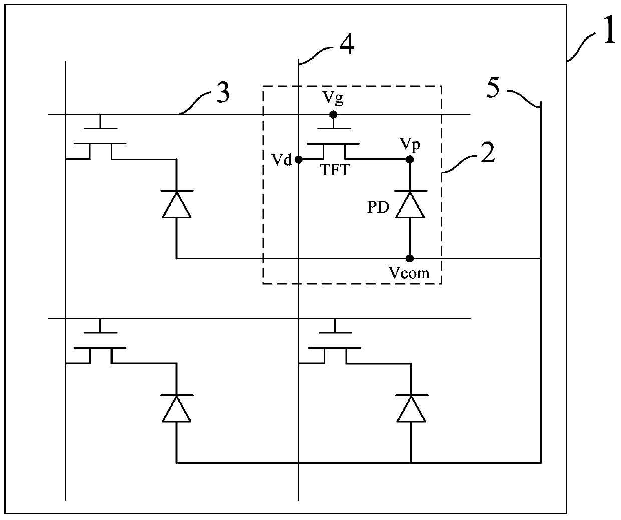
[0050] Such as figure 1 Shown is a schematic structural view of a flat panel detector, which includes pixel units 2 arranged in a two-dimensional array. In this embodiment, the pixel units 2 form an array of 2 rows and 2 columns. The pixel unit 2 includes a switch element and a photodiode PD. In this embodiment, the switch element is a thin film transistor TFT. The cathode of the photodiode PD is connected to the source of the thin film transistor TFT as a pixel electrode; the gates of the thin film transistors TFT located in the same row are connected to the same scanning line 3, and the gates of the thin film transistor TFT located in the same column The drains are connected to the same data line 4 , and the anodes of the photodiodes PD are connected to the common electrode 5 .

[0051] Such as Figure 4 Shown is the relationship between the source-drain current Ids and the gate-source voltage Vgs of a conventional N-type amorphous silicon thin film transistor (the figure...

Embodiment 2

[0064] The first embodiment takes an N-type thin film transistor as an example, and this method is also applicable to a P-type switching element. In this embodiment, a P-type thin film transistor is taken as an example, and its principle is basically the same as that of the embodiment, except that the N-type thin film transistor is replaced by a P-type thin film transistor.

[0065] The conduction characteristics of the P-type thin film transistor are as follows: when VgsVth, the thin film transistor is in an off state. In this embodiment, the potential Vcom of the common electrode 5 is a positive potential, taking 8V as an example.

[0066] Reset phase: the switching element is turned on by reducing the gate voltage of the switching element to perform a reset operation.

[0067] Waiting for exposure stage: reducing the gate potential of the switching element to a set potential, at which time the switching element is still in the off state, and the set potential is lower than...


PUM


Abstract

The invention provides a driving method for an image sensor, which includes: opening a switching element, releasing the residual signal in the pixel unit, and then closing the switching element; setting the gate potential of the switching element to a set potential, while the switching element is still In the off state; Read the line. During exposure, the present invention leaks excess charges, maintains a certain voltage difference at both ends of the photodiode, and defects do not capture electrons, so the problem of residual images can be fundamentally solved; in addition, after the exposure is completed, a certain line can be read out. At this time, by adjusting the gate voltage, the leakage current of the thin film transistors in other rows is at the lowest state, eliminating the crosstalk problem and greatly improving the image quality.

Description

technical field [0001] The invention relates to the technical field of semiconductors, in particular to a driving method of an image sensor. Background technique [0002] Flat panel image sensors are widely used in medical radiation imaging, industrial flaw detection, security inspection and other fields. Flat-panel image sensors, especially large-scale image sensors, have an area of ​​tens of centimeters and millions to tens of millions of pixels, usually using amorphous silicon technology. [0003] A flat-panel image sensor generally includes: a substrate 1 (may be glass or plastic, etc.), on which all sensors are placed; pixel units 2, which are arranged in a two-dimensional array on the substrate 1 Each pixel unit 2 includes a photodiode PD (PhotoDiode) and a thin film transistor TFT (Thin Film Transistor); used to control the scan line 3 and data line 4 of each pixel 2; and used to provide the photodiode PD Voltage common electrode 5. Applying a negative voltage (suc...

Claims


Application Information

Patent Timeline
Patent Type & Authority Patents(China)
IPC IPC(8): H04N5/335H04N5/359H04N25/00
Inventor 金利波郑金磊黄细平方志强
Owner SHANGHAI IRAY TECH
Features
  • Generate Ideas
  • Intellectual Property
  • Life Sciences
  • Materials
  • Tech Scout
  • Unparalleled Data Quality
  • Higher Quality Content
  • 60% Fewer Hallucinations
Learn More